CMS32L051 User Manual |Chapter 23 Voltage Detection Circuit
www.mcu.com.cn 651 / 703
23.3 Registers for controlling voltage detection circuit
The voltage detection circuit is controlled by the following registers.
Voltage Sense Register (LVIM).
Voltage Sense Level Register (LVIS).
23.3.1 Voltage sense register (LVIM).
This register setting enables or disables overriding the voltage sense register (LVIS) and confirms the
shielding status of the LVD output. The LVIM registers are set via 8-bit memory operation instructions.
After the reset signal is generated, the value of this register becomes 00H.
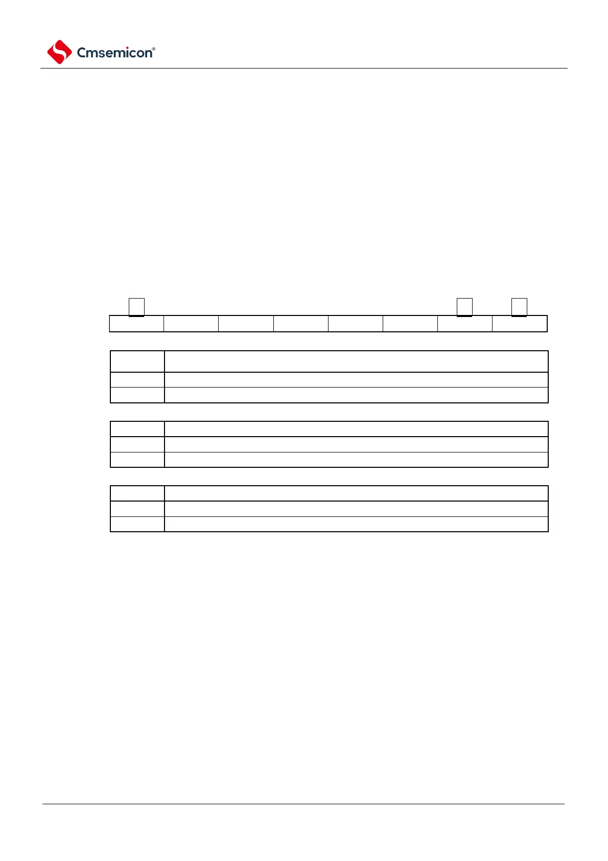
Figure 23-2 Format of voltage sense register (LVIM)
Address: 40020441H After reset: 00HNote
1
R/W
Note
2
symbol
LVIM
Enable/disable override setting for voltage sense level registers (LVIS).
It is forbidden to overwrite the LVIS register (LVIOMSK=0 (LVD output mask is invalid)).
Rewriting of LVIS registers (LVIOMSK=1 (LVD output masking active)) is Enableed.
Mask status flag of the LVD output
The LVD output mask is invalid.
LVD output shielding valid
Note
4
.
The supply voltage (V
DD)
LVD
) or LVD is OFF.
Supply voltage (V
DD
< sense voltage (V
LVD
)
Note 1. The reset value varies depending on the reset source.
When the LVD is reset, the value of the LVIM register is not reset and the original value is maintained; On
other resets, clear LVISEN to 0.
2. Bit0 and bit1 are read-only bits.
3. it can only be set when interrupt & reset mode is selected (the LVIMDS1 bit and LVIMDS0 bits of the option byte
are 1 and 0, respectively), and the initial value cannot be changed in other modes.
4. Only when the interrupt & reset mode is selected (the LVIMDS1 bit and LVIMDS0 bits of the option bytes are 1
and 0, respectively). The LVIOMSK bit automatically changes to 1 during the following periods, masking the
reset or interrupt caused by LVD.
period
time from the time the LVD interrupt occurs until the LVD sense voltage stabilizes
the value of the LVILV bit until the LVD sense voltage stabilizes