CMS32L051 User Manual |Chapter 11 A/D Converter
www.mcu.com.cn 275 / 703
11.2.4 A/D converter mode register 2 (ADM2)
The ADM2 register is set by 8-bit memory operation instructions.
After the reset signal is generated, the value of this register becomes 00H.
Figure11-6 Format of A/D converter mode register 2 (ADM2) (1/3)
Selection of positive (+) voltage references for A/D converters
Provided by internal reference voltage (1.45V).
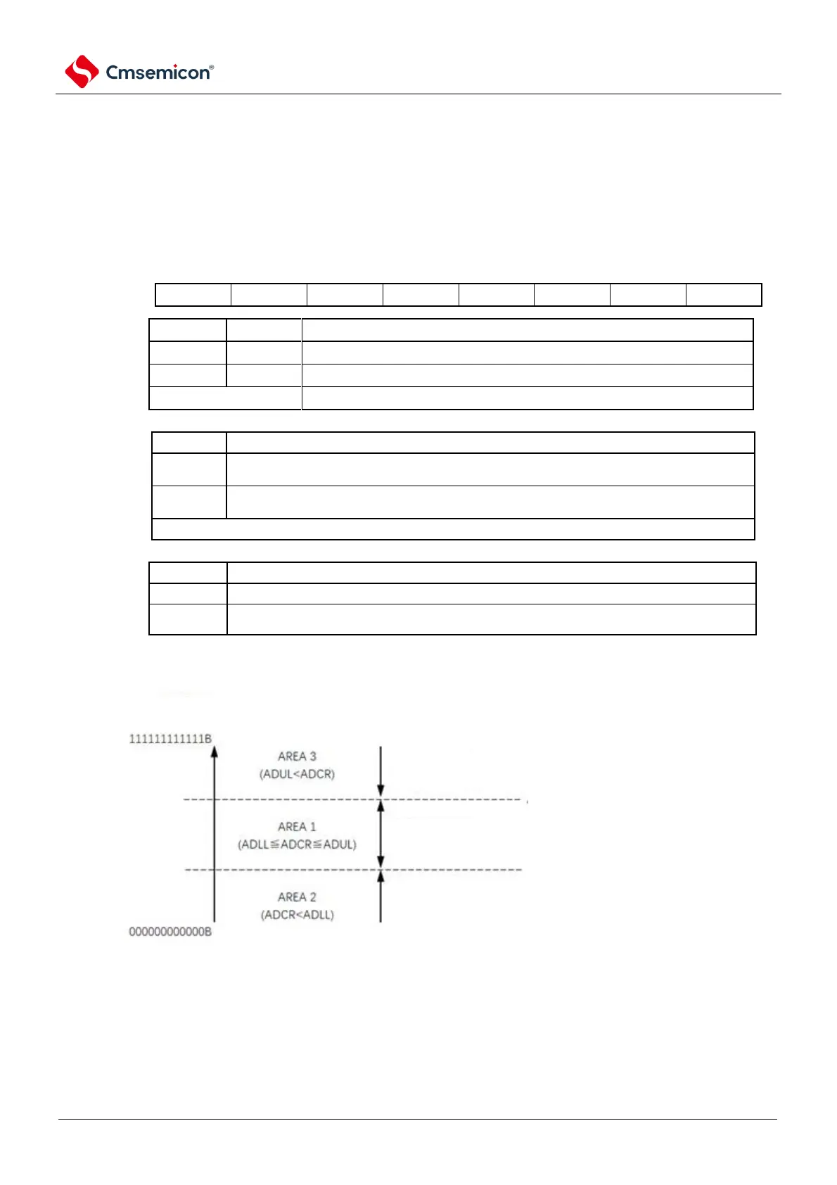
Check the upper and lower values of the conversion result
When the ADLL the ADCR ADUL register (AREA1), an interrupt signal
(INTAD) is generated.
When ADCRRegister <ADLLRegisters (AREA2OrADULTSRegister <ADCRRegisters
(AREA3), an interrupt signal is generated(INTAD).
The range of interrupt signal (INTAD) generated from AREA1 to AREA3 is shown in Figure 15-8.
The output of the channel identification is enabled when the A/D converter scans mode
When scanning mode, the channel number is not identified in the conversion results
When scanning mode, the high four bits of the converted result ([15:12] of the ADCR register)
are the channel numbers for this result
Figure11-7 Range of interrupt signal generation for the ADRCK bit
value in ADCR register
(A/D conversion result)
when ADRCK=1, generates
INTAD interrupt
when ADRCK=0, generates
INTAD interrupt
when ADRCK=1, generates
INTAD interrupt
configure value of ADUL register
configure value of ADLL register
Note 1 To override the ADM2 register, it must be done in the transition stop state (ADCS=0).
Note When INTAD does not occur, the A/D conversion results are not saved to the ADCR register and the ADCRH
register.