EasyManua.ls Logo

Cmsemicon CMS32L051 - SPI Clock Selection Register (SPIC)

Default Icon
703 pages
Print Icon
To Next Page IconTo Next Page
To Previous Page IconTo Previous Page
Loading...
V1.2.2
CMS32L051 User Manual |Chapter 13 Serial Interface SPI
www.mcu.com.cn 463 / 703
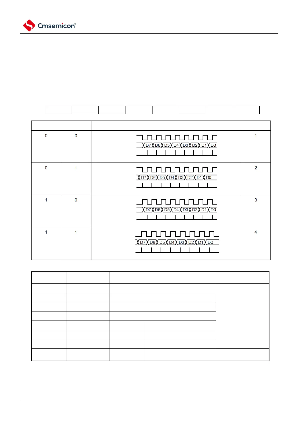
13.3.3 SPI clock selection register (SPIC)
This register specifies the timing of data sending/receiving and sets the serial clock.
It can be set by 8-bit storage operation instructions.
A reset signal is generated to clear the register to 00H.
Figure13-3 Format of clock selection register (SPIC)
Address: 0x40042404 After reset: 00HR/W
symbol
7
6
5
4
3
2
1
0
SPIC
0
0
0
CKP
Dap
CKS2
CKS1
CKS0
SCK
MISO/MOSI
(Output timing)
MISO/MOSI
(Input timing)
SCK
MISO/MOSI
(Output timing)
MISO/MOSI
(Input timing)
SCK
MISO/MOSI
(Output timing)
MISO/MOSI
(Input timing)
SCK
MISO/MOSI
(Output timing)
MISO/MOSI
(Input timing)
CKP DAP
TypeDesignation of data transmission/reception timing
CKS2
CKS1
CKS0
SPI serial clock selection
mode
0
0
0
fCLK
Master mode
0
0
1
fCLK/2
0
1
0
fCLK/2
2
0
1
1
fCLK/2
3
1
0
0
fCLK/2
4
1
0
1
fCLK/2
5
1
1
0
fCLK/2
6
1
1
1
The external clock entered
from the SCK
Slave mode
Note 1. Writing is disabled when SPPIE=1 (operation enable).
2. The phase type of the data clock after reset is type 1.

Table of Contents

Related product manuals