CMS32L051 User Manual |Chapter 1 CPU
www.mcu.com.cn 16 / 703
1.4 SWD interface pin
The two GPIOs of this product can be used as SWD interface pins, which are present in all packages.
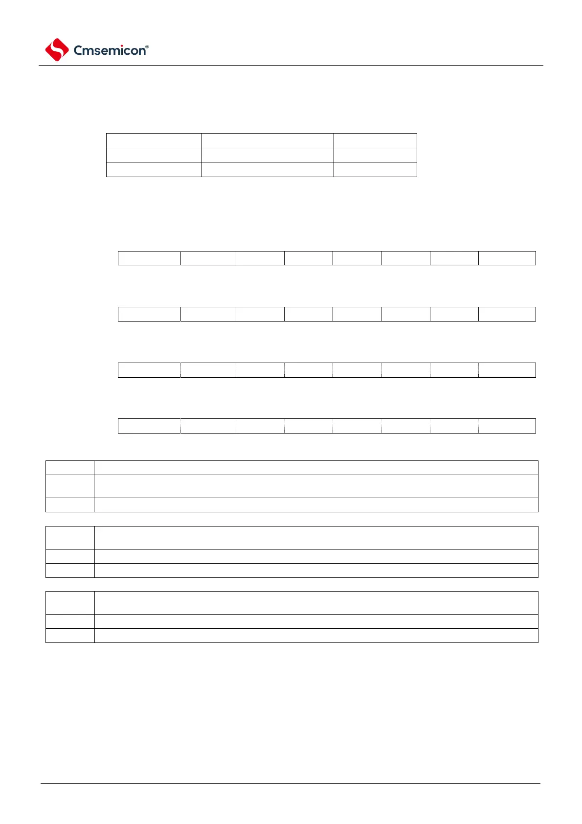
Table 1-1 SWD debug port pins
When the SWD function is not used, SWD can be disabled by setting the debug stop control register
(DBGSTOPCR).
SWD debug interface status
The SWD debug interface is enabled. P40 cannot be used as a GPIO when the debugger is
connected (because the ENO and DOUT of the IOBUF are controlled by the debugger at this time)
The SWD debug interface is disabled. The P40 can be used as a GPIO
In the state where the debugger is connected and the CPU is in the debug state (HALTED=1), the
timer is peripheral module action/stop
Note 1
In the state where the debugger is connected and the CPU is in the debug state (HALTED=1), the
communication system peripheral module action/stop
Note 2
Note 1: The timer peripheral modules of this product include: Timer4, a universal timer unit.
Note 2: The peripheral modules of the communication system of this product include: communication serial
communication unit, serial IICA.