CMS32L051 User Manual |Chapter 4 Clock Generation Circuit
www.mcu.com.cn 72 / 703
4.3.6 Peripheral enable registers 0, 1 (PER0, PER1).
This is the register that sets the clock that is allowed or disallowed for each peripheral hardware.
Reduce power consumption and noise by stopping clocking unused hardware.
When the following peripheral functions controlled by these registers are used, the corresponding
bit should be set to 1 before the initial setting of the peripheral function is performed.
•
Real-time clock, 15-bit interval timer
•
IrDA
•
A/D converter
•
Serial interface IICA0
•
Universal serial communication unit 1
•
Universal serial communication unit 0
•
General purpose timer unit 1
•
General purpose timer unit 0
•
D/A converter
•
Enhanced DMA
•
EPWM
•
SPI
The PER0 register and the PER1 register are set via 8-bit memory operation instructions.
After the reset signal is generated, the values of these registers become 00H.
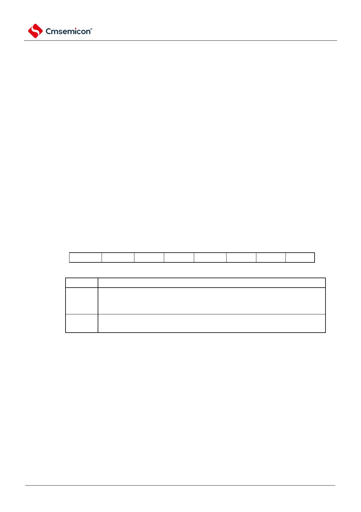
Figure 4-7 Format of peripheral enable register 0 (PER0) (1/3)
Address: 40020 420H After reset: 00H R/W
symbol
PER0
Stop supplying the input clock.
Cannot write the SFR used by the real-time clock (RTC) and 15-bit interval timer.
-time clock (RTC) and 15-bit interval timer are in the reset state.
An input clock is provided.
-time clock (RTC) and 15-bit interval timer.