CMS32L051 User Manual |Chapter 4 Clock Generation Circuit
www.mcu.com.cn 73 / 703
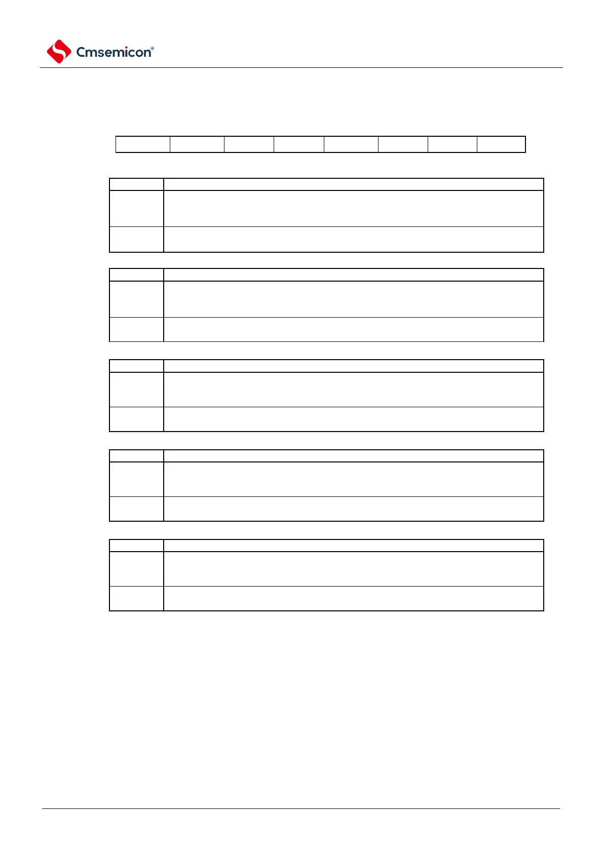
Figure 4-7 Format of peripheral enable register 0 (PER0) (2/3)
Address: 40020 420H After reset: 00H R/W
symbol
PER0
Provides control of the input clock of the serial interface IRDA
Stop supplying the input clock.
using SFR.
IRDA is in a reset state.
An input clock is provided.
used by I RDA.
Provides control of the input clock of the A/D converter
Stop supplying the input clock.
A/D converters using SFR.
An input clock is provided.
to A/D converters used.
Provides control of the input clock of the serial interface IICA0
Stop supplying the input clock.
serial interface IICA0 using SFR.
IICA0 is in a reset state.
An input clock is provided.
SFR used by the serial interface IICA0.
Provides control of the input clock of universal serial communication unit 1
Stop supplying the input clock.
1.
1 is in reset state.
An input clock is provided.
used by universal serial communication unit 1 can read and write.
Provides control of the input clock of universal serial communication unit 0
Stop supplying the input clock.
0.
Universal serial communication unit 0 is in a reset state.
An input clock is provided.
used by universal serial communication unit 0 can read and write.