CMS32L051 User Manual |Chapter 5 Universal Timer Unit (Timer4)
www.mcu.com.cn 145 / 703
(2) Selecting the active edge of the TImn pin input signal (CCSmn=1)
The Count Clock (fTCLK) is the signal that detects the active edge of the input signal of the TImn pin
and synchronizes it with the rising edge of the next fMCK. In fact, this is a signal that is delayed by 1 to 2
fMCK clocks than the input signal at the TImn pin (3 to 4 when using noise filters). fMCK clocks). To obtain
synchronization with fCLK, the timer count register mn (TCRmn) counts after delaying 1 fCLK from the
rising edge of the count clock. For convenience, it is called counting on the effective edge of the input
signal at the TImn pin.
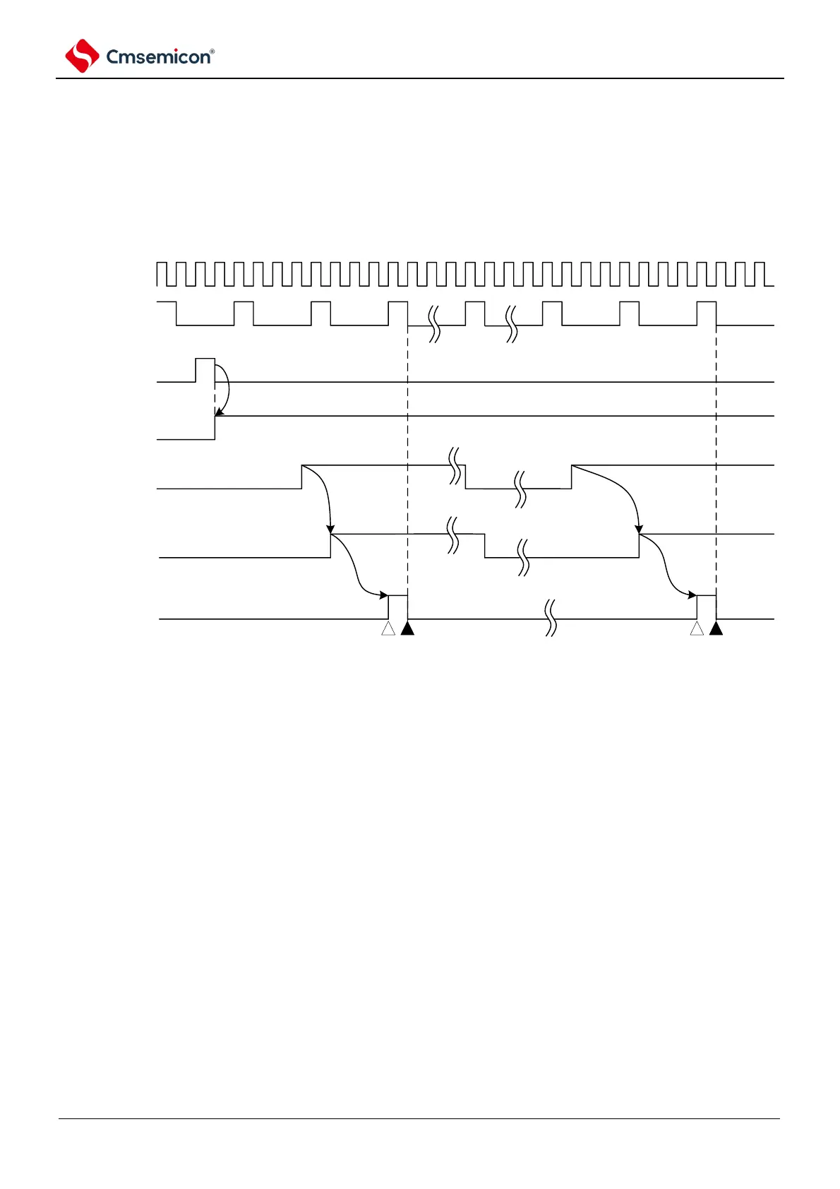
Figure 5-25 Count Clock (f
TCLK
) (CCSmn=1, without noise filter)
(1) Start the operation of the timer by placing the TSmn position bit, and wait for the valid edge of the TImn
input.
(2) Sample the rising edge of the TImn input through f
MCK
.
(3) The edge is detected on the rising edge of the sampled signal, and the detection signal
(counting clock) is output.
Note 1 △: Counts the rising edge of the clock
2.f
CLK
: CPU peripheral hardware clock
f
MCK
: The operating clock for channel n
3. The same waveform is used for the measurement of the input pulse interval, the measurement of the high and low levels of
the input signal, the delay counter, and the TImn input for the single-trigger pulse output function.