CMS32L051 User Manual |Chapter 5 Universal Timer Unit (Timer4)
www.mcu.com.cn 178 / 703
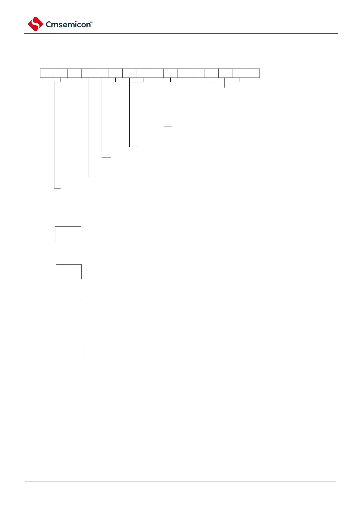
Figure 5-56 Example of register settings when measuring the high and low level widths of an input signal
(a) Timer mode register mn (TMRmn).
CKSmn1
1/0
CKSmn0
0
0
CCSmn
0
M/S
Note
0
STSmn2
0
STSmn1
1
STSmn0
0
CISmn1
1
CISmn0
1/0
0 0
MDmn3
1
MDmn2
1
MDmn1
0
MDmn0
0
14 13 12 11 10 9 8 7 6 5 4 3 2 1 015
TMRmn
operation mode of Channel N
110B:capture & single counting
operation configuration when start counting
0: when start counting, not to generate INTTMmn and do not generate inverted Phase Timer output.
start trigger selection
010B: Select Timn pin input valid edge
MASTERmn bit configuration (Channel 2)
0: Independent Channel operation
SPLITmn bit configuration (Channel 1, 3)
0: 16 bit Timer
Count clock selection
0: Select operational clock (fMCK)
operational clock (fMCK) selection
00B: select CKm0 as operational clock of Channel n
10B: select CKm1 as operational clock of Channel n.
01B: select CKm2 as operational clock of Channel 1,3.(only Channle 1,3 can select the value)
11B: select CKm3 as operational clock of Channel 1,3.(only Channle 1,3 can select the value)
Timn Pin input edge selection
10B:selection both edges (measure low voltage width)
11B:selection both edges (measure High voltage width)
Note: TMRm2: MASTERmn bit
TMRm1, TMRm3: SPLITmn bit
TMRm0: Fixed to 0.
Remark: m: Unit number (m=0) n: Channel number (n=0 ~ 3).