CMS32L051 User Manual |Chapter 12 Universal Serial Communication Unit
www.mcu.com.cn 344 / 703
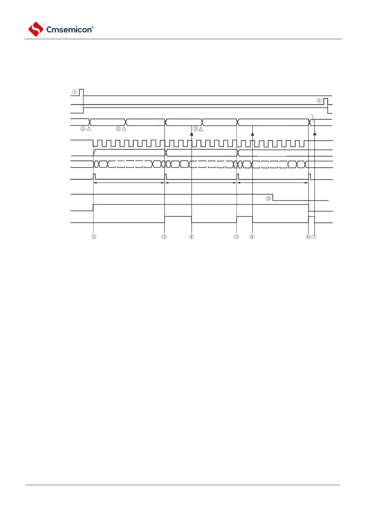
(4) Process flow (continuous receive mode).
Figure 12-37 Timing diagram of the master receive (continuous receive mode)
(type 1: DAPmn=0, CKPmn=0).
SCLKp pin
SDIp pin
INTSSPIp
shift register mn
TSFmn
SDRmn
SEmn
STmn
SSmn
BFFmn
MDmn0
virtual data virtual data virtual data
data reception2
data reception3
data reception3
data reception2
data reception2
data reception data reception data reception
Receiving&shift operation
data reception1
Receiving&shift operation
Receiving&shift operation
Read
Write
Read
Read
Write
Write
Note The MDmn0 bit can be overridden even during operation. However, in order to catch up with the end of
transmission interruption of the last received data, it must be overridden before the last bit of reception begins.
Note 1 (1) ~ (8) in the figure corresponds to (1) ~ (8) in the flowchart of theFigure 12-381238.
2.m: Unit number (m=0, 1)n: Channel number (n=0~3)p: SSPI number (p=00, 01, 10, 11, 20, 21)
mn=00~03, 10~11