CMS32L051 User Manual |Chapter 12 Universal Serial Communication Unit
www.mcu.com.cn 438 / 703
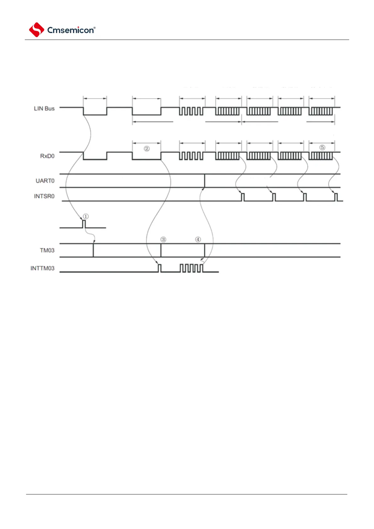
A summary of the receive operation of LIN is shown in Figure 12-115.
Figure 12-115 Receive operation of LIN
wake up
signal frame
interval field sync field identifier data field checksumdata field
BF reception SF reception ID reception
Stop stop receiving
Stop measurement pulse width
measurement
pulse width
measurement
pulse width
edge detection
(INTP0)
Data
reception
Data
reception
Data
reception
header
information
The flow of signal processing is as follows:
(1) The wake-up signal is detected by detecting the interrupt edge (INTP0) of the pin. When a wake-up
signal is detected, in order to measure the low-level width of BF, TM03 is set to measure the pulse
width and then enters the BF receive wait state.
(2) If a falling edge of BF is detected, TM03 begins measuring the width of the low level and snaps at the
rising edge of BF. Determine whether it is a BF signal based on the captured value.
(3) When BF reception ends normally, TM03 must be set to measure pulse intervals, and the interval
between the falling edges of the RxD0 signal in the 4th sync field must be measured (see 5.8.4
Operation as input pulse interval measurements).
(4) The baud rate error is calculated based on the bit interval of the sync field (SF). The baud rate must
then be adjusted (reset) after pausing UART0 operation.
(5) The checksum field must be distinguished by software. UART0 must also be initialized by software
after receiving the checksum field and set again to the BF receive wait state.