CMS32L051 User Manual |Chapter 12 Universal Serial Communication Unit
www.mcu.com.cn 440 / 703
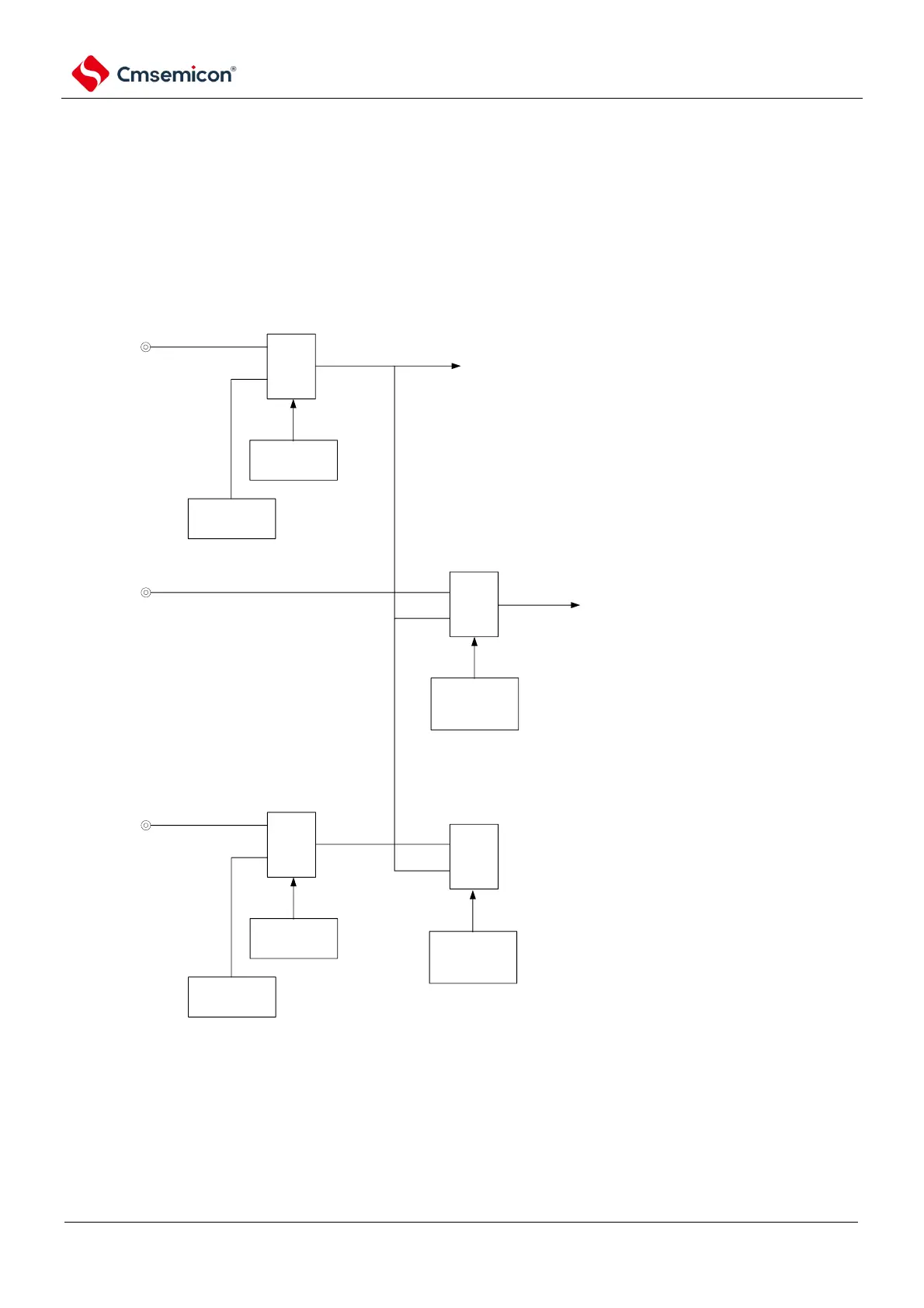
The port structure diagram for LIN receive operation is shown in Figure 12-117.
The wake-up signal sent by the LIN master is received by the edge detection of the external interrupt
(INTP0). It can be operated by external event capture of the universal timer unit, measuring the length of the
synchronization segment sent by the LIN master and calculating the baud rate error.
With port input switching control (ISC0/ISC1), the input source for the received port input (RxD0) can be
input to the external interrupt (INTP0) and timer array unit without external wiring.
Figure 12-117 Port block diagram for LIN receive operation
port mode
(PMxx)
Pxx/RxD0
output latch
(Pxx)
RxD0 input
selector
selector
Pxx/INTP0
INTP0 input
port input
switch control
(ISC0)
selector
port mode
(PMxx)
Pxx/TI03
output latch
(Pxx)
selector
<ISC0>
0: set INTP0 pin input signal as external interrupt input
1: set RxD0 pin input singal as external interrupt input
port input
switch control
(ISC1)
<ISC0>
0: set TI03 pin input singal as universal timer unit0 channel 3 input
1: set RxD0 pin input signal as universal timer unit 0 channel 3 input