RM0453 Rev 1 133/1461
RM0453 Embedded Flash memory (FLASH)
153
4.10.6 FLASH control register (FLASH_CR)
Address offset: 0x014
Reset value: 0xC000 0000
Access: no wait state when no Flash memory operation is ongoing. Word, half-word and
byte access.
This register cannot be modified when CFGBSY is set in FLASH_SR.
When PESD is cleared in FLASH_SR, the register write access is stalled until the CFGBSY
bit is cleared (for example by the other CPU).
When PESD is set in FLASH_SR and a program or an erase operation is ongoing, the
register write access causes a bus error.
When PESD is set in FLASH_SR but there is no ongoing programming or erase operation,
the register write access is completed, but the requested operation is suspended.
BSY/CFGBSY is set and remains 1 until suspend is deactivated by clearing the PES bits in
FALSH_ACR and FLASH_C2ACR. Consequently PESD goes back to 0 and the suspended
operation completes.
Bit 2 Reserved, must be kept at reset value.
Bit 1 OPERR: Operation error
This bit is set by hardware when a Flash memory operation (program/erase) completes
unsuccessfully. This bit is set only if error interrupts are enabled (ERRIE = 1).
This bit is cleared by writing 1.
Bit 0 EOP: End of operation
This bit is set by hardware when one or more Flash memory operation (program/erase)
completes successfully. This bit is set only if the end of operation interrupts are enabled
(EOPIE = 1).
This bit is cleared by writing 1.
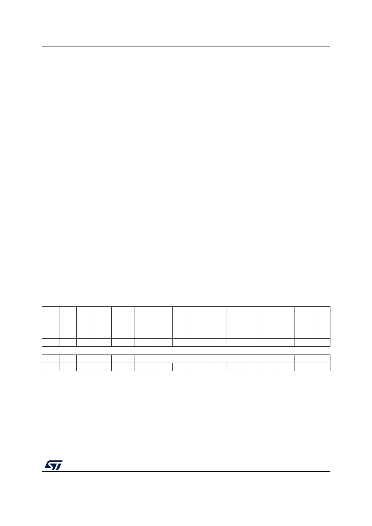
31 30 29 28 27 26 25 24 23 22 21 20 19 18 17 16
LOCK
OPTLOCK
Res. Res.
OBL_LAUNCH
RDERRIE
ERRIE EOPIE Res. Res. Res. Res. Res. FSTPG
OPTSTRT
STRT
rs rs rc_w1 rw rw rw rw rs rs
15 14 13 12 11 10 9 8 7 6 5 4 3 2 1 0
Res. Res. Res. Res. Res. Res. PNB[6:0] MER PER PG
rw rw rw rw rw rw rw rw rw rw

 Loading...


