Digital-to-analog converter (DAC) RM0453
616/1461 RM0453 Rev 1
19.7.14 DAC sample and hold time register (DAC_SHHR)
Address offset: 0x48
Reset value: 0x0001 0001
Note: These bits can be written only when the DAC channel is disabled and in Normal operating
mode (when bit EN1=0 and bit CEN1=0 in the DAC_CR register). If EN1=1 or CEN1=1 the
write operation is ignored.
19.7.15 DAC sample and hold refresh time register (DAC_SHRR)
Address offset: 0x4C
Reset value: 0x0001 0001
Note: These bits can be written only when the DAC channel is disabled and in Normal operating
mode (when bit EN1=0 and bit CEN1=0 in the DAC_CR register). If EN1=1 or CEN1=1 the
write operation is ignored.
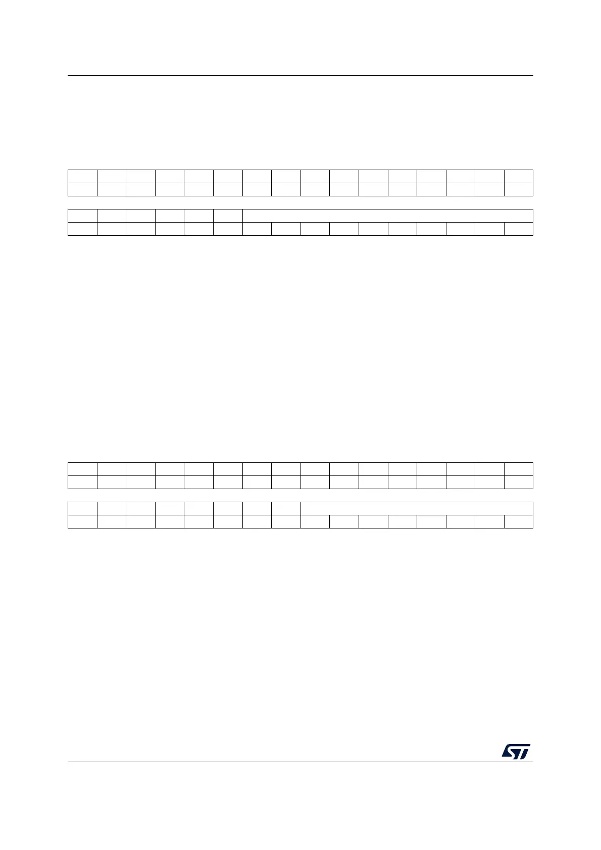
31 30 29 28 27 26 25 24 23 22 21 20 19 18 17 16
Res. Res. Res. Res. Res. Res. Res. Res. Res. Res. Res. Res. Res. Res. Res. Res.
1514131211109876543210
Res. Res. Res. Res. Res. Res. THOLD1[9:0]
rw rw rw rw rw rw rw rw rw rw
Bits 31:16
Reserved, must be kept at reset value.
Bits 15:10 Reserved, must be kept at reset value.
Bits 9:0 THOLD1[9:0]: DAC channel1 hold time (only valid in Sample and hold mode)
Hold time= (THOLD[9:0]) x LSI clock period
Note: This register can be modified only when EN1=0.
31 30 29 28 27 26 25 24 23 22 21 20 19 18 17 16
Res. Res. Res. Res. Res. Res. Res. Res. Res. Res. Res. Res. Res. Res. Res. Res.
1514131211109876543210
Res. Res. Res. Res. Res. Res. Res. Res. TREFRESH1[7:0]
rw rw rw rw rw rw rw rw
Bits 31:16
Reserved, must be kept at reset value.
Bits 15:8 Reserved, must be kept at reset value.
Bits 7:0 TREFRESH1[7:0]: DAC channel1 refresh time (only valid in Sample and hold mode)
Refresh time= (TREFRESH[7:0]) x LSI clock period
Note: This register can be modified only when EN1=0.

 Loading...


