Digital-to-analog converter (DAC) RM0453
598/1461 RM0453 Rev 1
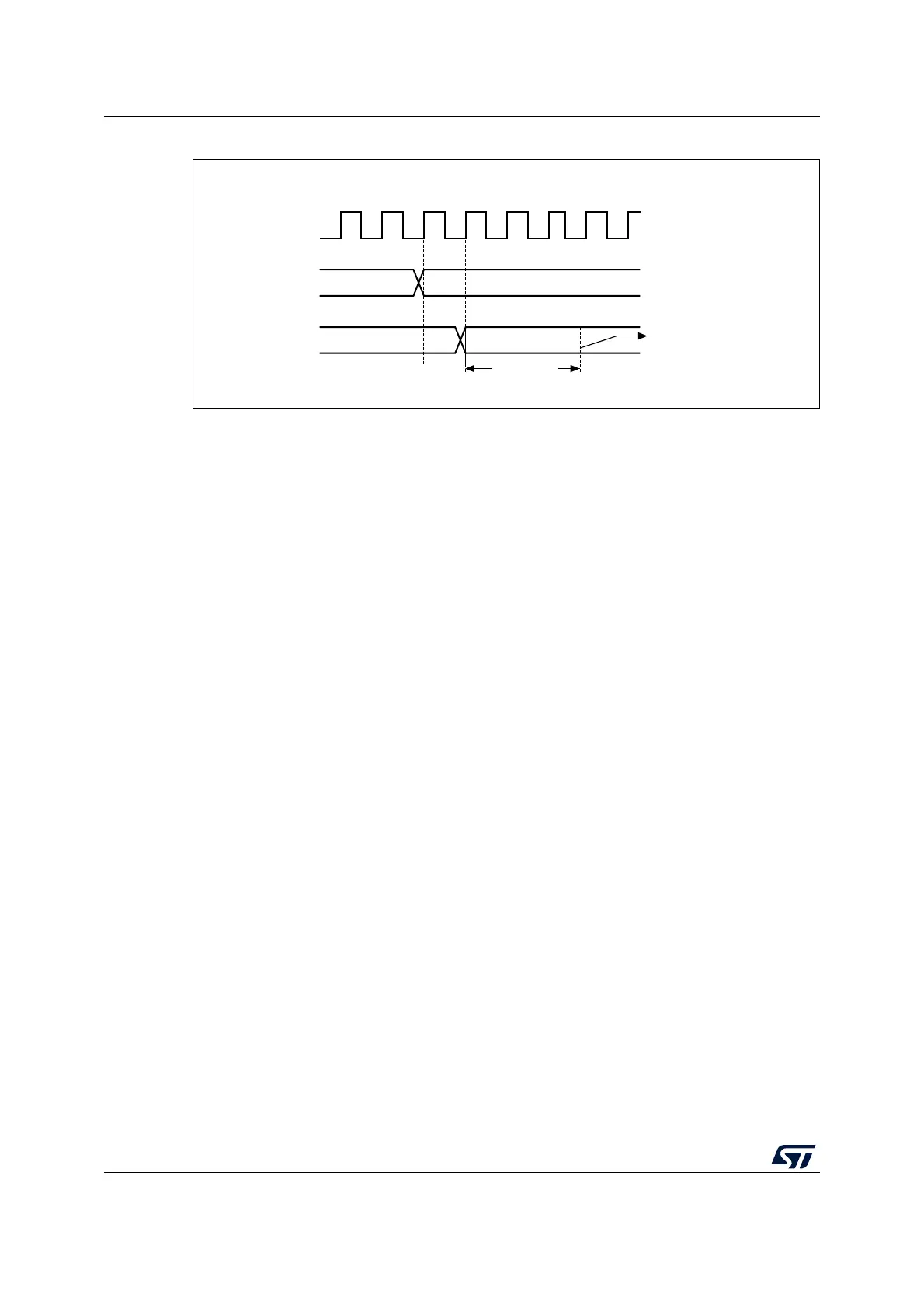
Figure 88. Timing diagram for conversion with trigger disabled TEN = 0
19.4.6 DAC output voltage
Digital inputs are converted to output voltages on a linear conversion between 0 and V
REF+
.
The analog output voltage on the DAC channel pin is determined by the following equation:
19.4.7 DAC trigger selection
If the TEN1 control bit is set, the conversion can then be triggered by an external event (timer
counter, external interrupt line). The TSEL1[3:0] control bits determine which out of 16 pos-
sible events triggers the conversion as shown in TSEL1[3:0] bits of the DAC_CR register.
These events can be either the software trigger or hardware triggers. Refer to the intercon-
nection table in Section 19.4.2: DAC pins and internal signals.
Each time a DAC interface detects a rising edge on the selected trigger source (refer to the
table below), the last data stored into the DAC_DHR1 register are transferred into the
DAC_DOR1 register. The DAC_DOR1 register is updated three dac_pclk cycles after the
trigger occurs.
If the software trigger is selected, the conversion starts once the SWTRIG bit is set.
SWTRIG is reset by hardware once the DAC_DOR1 register has been loaded with the
DAC_DHR1 register contents.
Note: TSEL1[3:0] bit cannot be changed when the EN1 bit is set.
When software trigger is selected, the transfer from the DAC_DHR1 register to the
DAC_DOR1 register takes only one dac_pclk clock cycle.
19.4.8 DMA requests
The DAC channel has a DMA capability. One DMA channel is used to service DAC channel
DMA request.
When an external trigger (but not a software trigger) occurs while the DMAEN1 bit is set, the
value of the DAC_DHR1 register is transferred into the DAC_DOR1 register when the
transfer is complete, and a DMA request is generated.
As DAC_DHR1 to DAC_DOR1 data transfer occurred before the DMA request, the very first
data has to be written to the DAC_DHR1 before the first trigger event occurs.
MSv45319V2
Bus clock
0x1AC
0x1AC
tSETTLING
DHR
DOR
Output voltage available on
DAC_OUT pin
DACoutput V
REF
DOR
4096
--------------
×=

 Loading...


