RM0453 Rev 1 1331/1461
RM0453 Debug support (DBG)
1448
Data registers are described in more detail in the Arm
®
Debug Interface Architecture
Specification [1].
38.3.9 Serial-wire debug port
The Serial-wire debug (SWD) protocol uses the two following pins:
• SWCLK: clock from host to target
• SWDIO: bi-directional serial data (100 kΩ pull-up required)
Serial data is transferred LSB first, synchronously with the clock.
Each transfer comprises the three phases listed below:
1. a packet request (8 bits) transmitted by the host (see Table 264)
2. an acknowledge response (3 bits) transmitted by the target (see Table 265)
3. data transfer (33 bits) transmitted by the host (in case of a write) or by the target (in
case of a read) (see
Table 266)
The data transfer only occurs if the acknowledge response is OK.
Between each phase, if the direction of the data is reversed, a single clock cycle
turn-around time is inserted.
1110 IDCODE 32
ID code
0x6BA0 0477: Arm
®
JTAG debug port ID code
1111 BYPASS 1
Bypass
A single JTCK cycle delay is inserted between JTDI and JTDO.
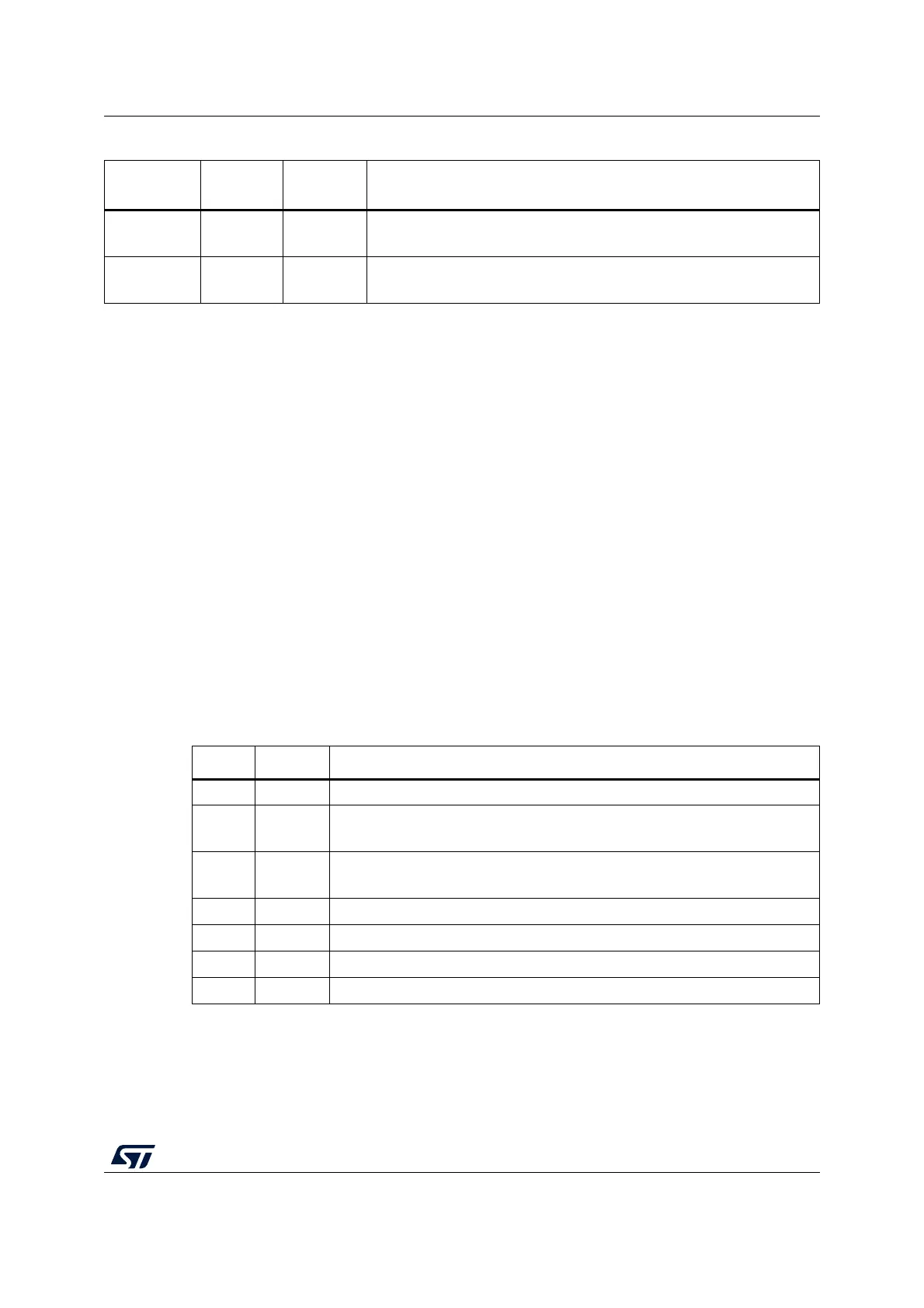
Table 263. JTAG-DP data registers (continued)
IR
instruction
Data
register
Scan chain
length
Description
Table 264. Packet request
Bit field Name Description
0 Start Must be 1.
1 APnDP
– 0: DP register access - see Table 263 for a list of DP registers
– 1: AP register access - see Section 38.5: Access ports
2RnW
– 0: Write request
– 1: Read request
4:3 A(3:2) Address field of the DP or AP registers
5 Parity Single bit parity of preceding bits
6Stop0
7 Park Not driven by host, must be read as 1 by the target.
 Loading...


