Debug support (DBG) RM0453
1342/1461 RM0453 Rev 1
38.5 Access ports
As shown in Figure 385, there are twois one access ports (AP) attached to the DP:
• AP0, CPU1 (Cortex-M4) access port (AHB-AP): enables access to the debug and trace
features integrated in the core via its internal AHB bus.
• AP1, CPU2 (Cortex-M0+) access port (AHB-AP): enables access to the debug and
trace features integrated in the core via its internal AHB bus.
The access ports are of MEM-AP type, that is to say the debug and trace component
registers are mapped in the address space of the associated debug bus.
AP is seen by the debugger as a set of 32-bit registers organized in banks of four registers
each. Some of these registers are used to configure or monitor the AP itself, while others
are used to perform a transfer on the bus.
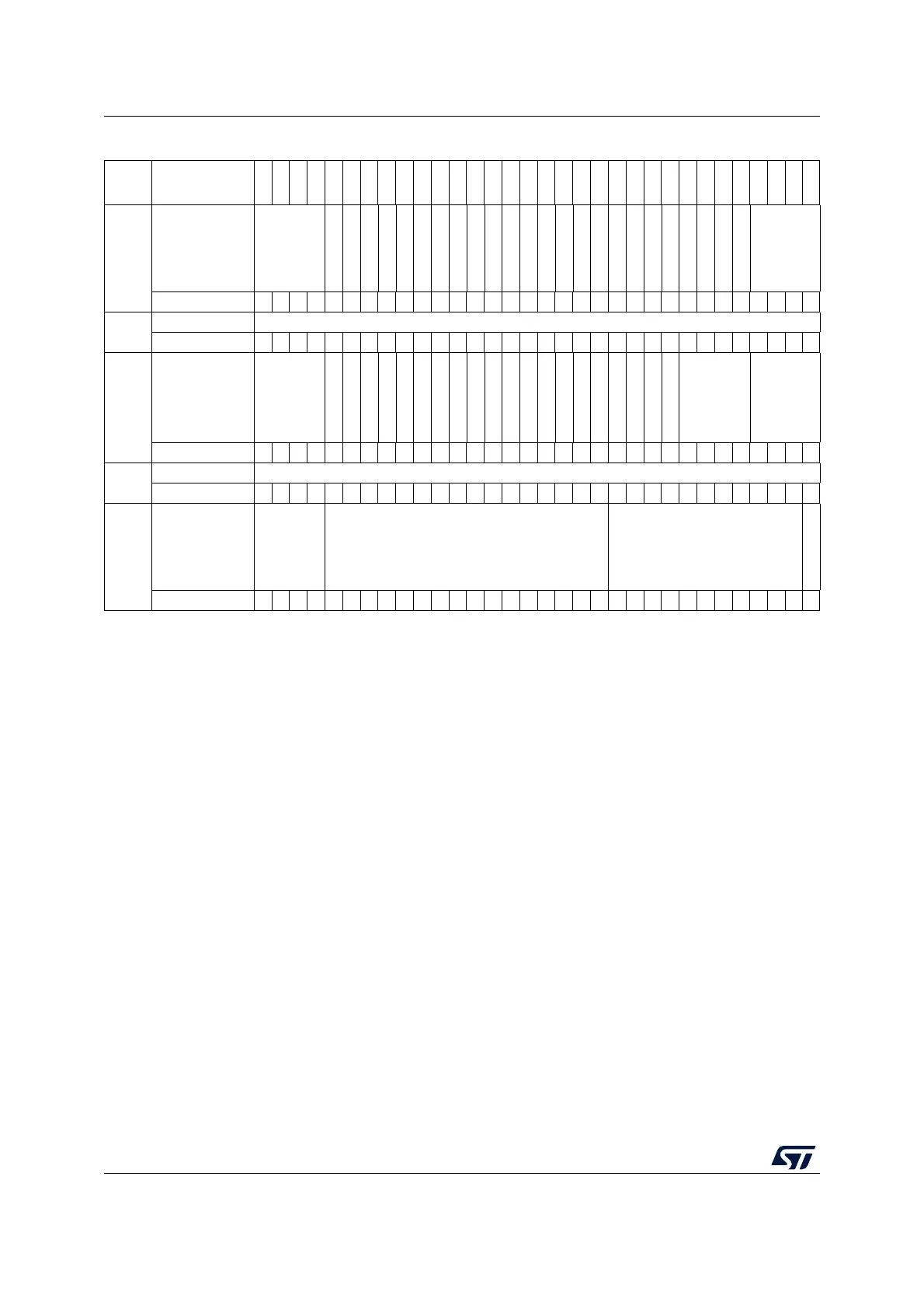
The AP registers are listed in Table 270: AP register map and reset values.
0x04
(4)
DP_DLPIDR
TINSTANCE[3:0]
Res.
Res.
Res.
Res.
Res.
Res.
Res.
Res.
Res.
Res.
Res.
Res.
Res.
Res.
Res.
Res.
Res.
Res.
Res.
Res.
Res.
Res.
Res.
Res.
PROTSVN[3:0]
Reset value 0000 0001
0x08
DP_RESENDR RESEND[31:0]
Reset value 00000000000000000000000000000000
0x08
DP_SELECTR APSEL[3:0]
Res.
Res.
Res.
Res.
Res.
Res.
Res.
Res.
Res.
Res.
Res.
Res.
Res.
Res.
Res.
Res.
Res.
Res.
Res.
Res.
APBANKSEL[3:0]
DPBANKSEL[3:0]
Reset value x x x x xxxxxxxx
0x0C
DP_BUFFR RDBUFF[31:0]
Reset value 00000000000000000000000000000000
0x0C
DP_TARGETSELR
TINSTANCE[3:0]
TPARTNO[15:0] TDESIGNER[10:0]
Res.
Reset value xxxxxxxxxxxxxxxxxxxxxxxxxxxxxxx
1. DP_SELECTR.DPBANKSEL = 0.
2. DP_SELECTR.DPBANKSEL = 1.
3. DP_SELECTR.DPBANKSEL = 2.
4. DP_SELECTR.DPBANKSEL = 3.
Table 268. DP register map and reset values (continued)
Offset Register name
31
30
29
28
27
26
25
24
23
22
21
20
19
18
17
16
15
14
13
12
11
10
9
8
7
6
5
4
3
2
1
0

 Loading...


