Embedded Flash memory (FLASH) RM0453
112/1461 RM0453 Rev 1
Programming and caches
If a Flash memory write access impacts data in the data cache, the Flash memory write
access modifies the data in the memory and in the cache.
If an erase operation in the Flash memory also concerns data in the data cache or
instruction cache, the user must ensure that these data are rewritten before they are
accessed during code execution. Upon an erase operation, the cache content is invalidated.
Note: The ICache and DCache must be flushed only when disabled (ICEN or DCEN = 0).
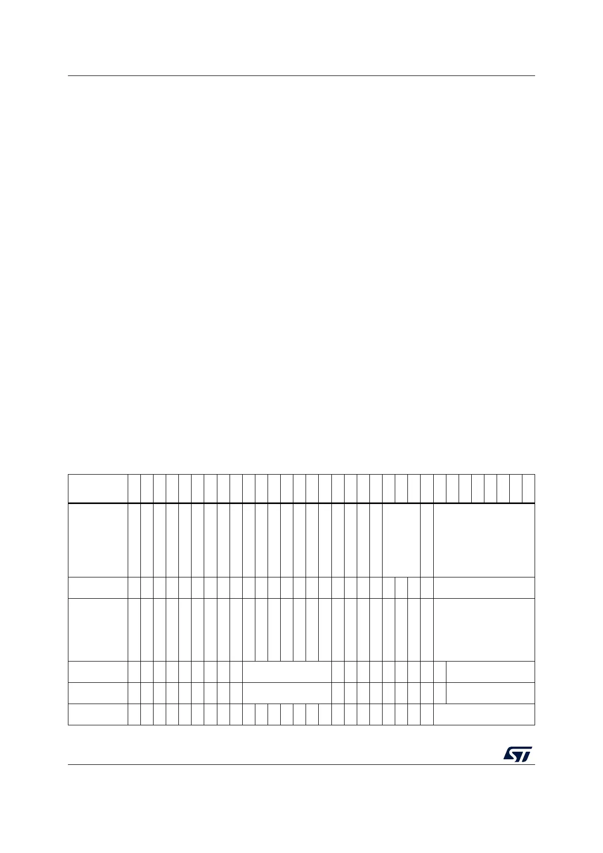
4.4 FLASH option bytes
4.4.1 Option bytes description
The option bytes can be read from the memory locations listed in the table below or from the
following option byte registers:
• FLASH option register (FLASH_OPTR)
• FLASH PCROP zone A start address register (FLASH_PCROP1ASR)
• FLASH PCROP zone A end address register (FLASH_PCROP1AER)
• FLASH PCROP zone B start address register (FLASH_PCROP1BSR)
• FLASH PCROP zone B end address register (FLASH_PCROP1BER)
• FLASH WRP area A address register (FLASH_WRP1AR)
• FLASH WRP area B address register (FLASH_WRP1BR)
• FLASH IPCC mailbox data buffer address register (FLASH_IPCCBR)
• FLASH CPU2 access control register (FLASH_C2ACR)
• FLASH secure SRAM start address and CPU2 reset vector register (FLASH_SRRVR)
Table 16. Option bytes organization
Address
(1)
31
30
29
28
27
26
25
24
23
22
21
20
19
18
17
16
15
14
13
12
11
10
9
8
7
6
5
4
3
2
1
0
0x1FFF 7800
C2BOOT_LOCK
BOOT_LOCK
Res.
Res.
nBOOT0
nSWBOOT0
SRAM_RST
SRAM2PAR
nBOOT1
Res.
Res.
Res.
WWDG_SW
IWDG_STDBY
IWDG_STOP
IWDG_SW
Res.
nRST_SHDW
nRST_STDBY
nRST_STOP
BOR_LEV[2:0]
ESE
RDP[7:0]
0x1FFF 7808
Res.
Res.
Res.
Res.
Res.
Res.
Res.
Res.
Res.
Res.
Res.
Res.
Res.
Res.
Res.
Res.
Res.
Res.
Res.
Res.
Res.
Res.
Res.
Res.
PCROP1A_STRT[7:0]
0x1FFF 7810
PCROP_RDP
Res.
Res.
Res.
Res.
Res.
Res.
Res.
Res.
Res.
Res.
Res.
Res.
Res.
Res.
Res.
Res.
Res.
Res.
Res.
Res.
Res.
Res.
Res.
PCROP1A_END[7:0]
0x1FFF 7818
Res.
Res.
Res.
Res.
Res.
Res.
Res.
Res.
Res.
WRP1A_END[6:0]
Res.
Res.
Res.
Res.
Res.
Res.
Res.
Res.
Res.
WRP1A_STRT[6:0]
0x1FFF 7820
Res.
Res.
Res.
Res.
Res.
Res.
Res.
Res.
Res.
WRP1B_END[6:0]
Res.
Res.
Res.
Res.
Res.
Res.
Res.
Res.
Res.
WRP1B_STRT[6:0]
0x1FFF 7828
Res.
Res.
Res.
Res.
Res.
Res.
Res.
Res.
Res.
Res.
Res.
Res.
Res.
Res.
Res.
Res.
Res.
Res.
Res.
Res.
Res.
Res.
Res.
Res.
PCROP1B_STRT[7:0]

 Loading...


