RM0453 Rev 1 1393/1461
RM0453 Debug support (DBG)
1448
38.9.2 FPB remap register (FPB_REMAPR)
Address offset: 0x004
Reset value: 0x2000 0000
38.9.3 FPB comparator register x (FPB_COMPxR)
Address offset: 0x008 + 0x004 * x, (x = 0 to 7)
Reset value: 0x0000 0000
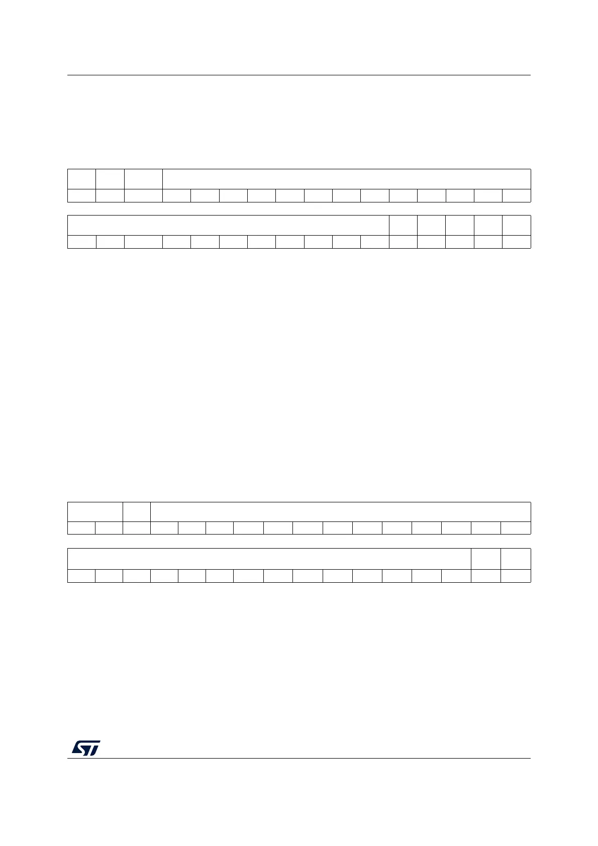
31 30 29 28 27 26 25 24 23 22 21 20 19 18 17 16
Res. Res.
RMPSPT REMAP[23:11]
r rwrwrwrwrwrwrwrwrwrwrwrwrw
1514 13 1211109876543210
REMAP[10:0]
Res. Res. Res. Res. Res.
rw rw rw rw rw rw rw rw rw rw rw
Bits 31:30 Reserved, must be kept at reset value.
Bit 29 RMPSPT: Flash memory patch remap
Indicates whether Flash memory patch remap is supported (read only).
1: Remapping supported.
Bits 28:5 REMAP[23:0]: remap target address
Bits [28:5] of the base address in SRAM to which the FPB remaps the address. The remap
base address must be aligned to the number of words required to support the implemented
comparators, that is to (NUM_CODE+NUM_LIT) words, with a minimum alignment of 8
words. Because remap is into the SRAM memory region, 0x20000000-0x3FFFFFFF, bits
[31:29] of the remap address are 0b001.
Bits 4:0 Reserved, must be kept at reset value.
31 30 29 28 27 26 25 24 23 22 21 20 19 18 17 16
REPLACE[1:0] Res.
COMP[26:14]
rw rw rw rw rw rw rw rw rw rw rw rw rw rw rw
15 14 13 12 11 10 9 8 7 6 5 4 3 2 1 0
COMP[13:0]
Res.
ENABL
E
rw rw rw rw rw rw rw rw rw rw rw rw rw rw rw

 Loading...


