Embedded Flash memory (FLASH) RM0453
130/1461 RM0453 Rev 1
4.10.3 FLASH key register (FLASH_KEYR)
Address offset: 0x008
Reset value: 0x0000 0000
s
4.10.4 FLASH option key register (FLASH_OPTKEYR)
Address offset: 0x00C
Reset value: 0x0000 0000
s
Bits 31:3 Reserved, must be kept at reset value.
Bit 2 C2SWDBGEN: CPU2 software debug enable
This bit is set and reset by software.
When HDPAD = 0 (hide protection area enabled), the CPU2 software debug is disabled after
a system reset.
When HDPAD = 1 (hide protection area disabled), the CPU2 software debug is enabled after
a system reset.
0: CPU2 debug access disabled
1: CPU2 debug access enabled (when also enabled in DDS)
Bit 1 HDPADIS: Flash user hide protection area access disable
This bit is set by software and is only reset by hardware on a system reset.
0: User Flash hide protection area access enabled
1: User Flash hide protection area access disabled
Bit 0 PRIVMODE: FLASH privileged mode enable
This bit is set and reset by software.
0: FLASH register access privileged mode disabled
1: FLASH register access privileged mode enabled
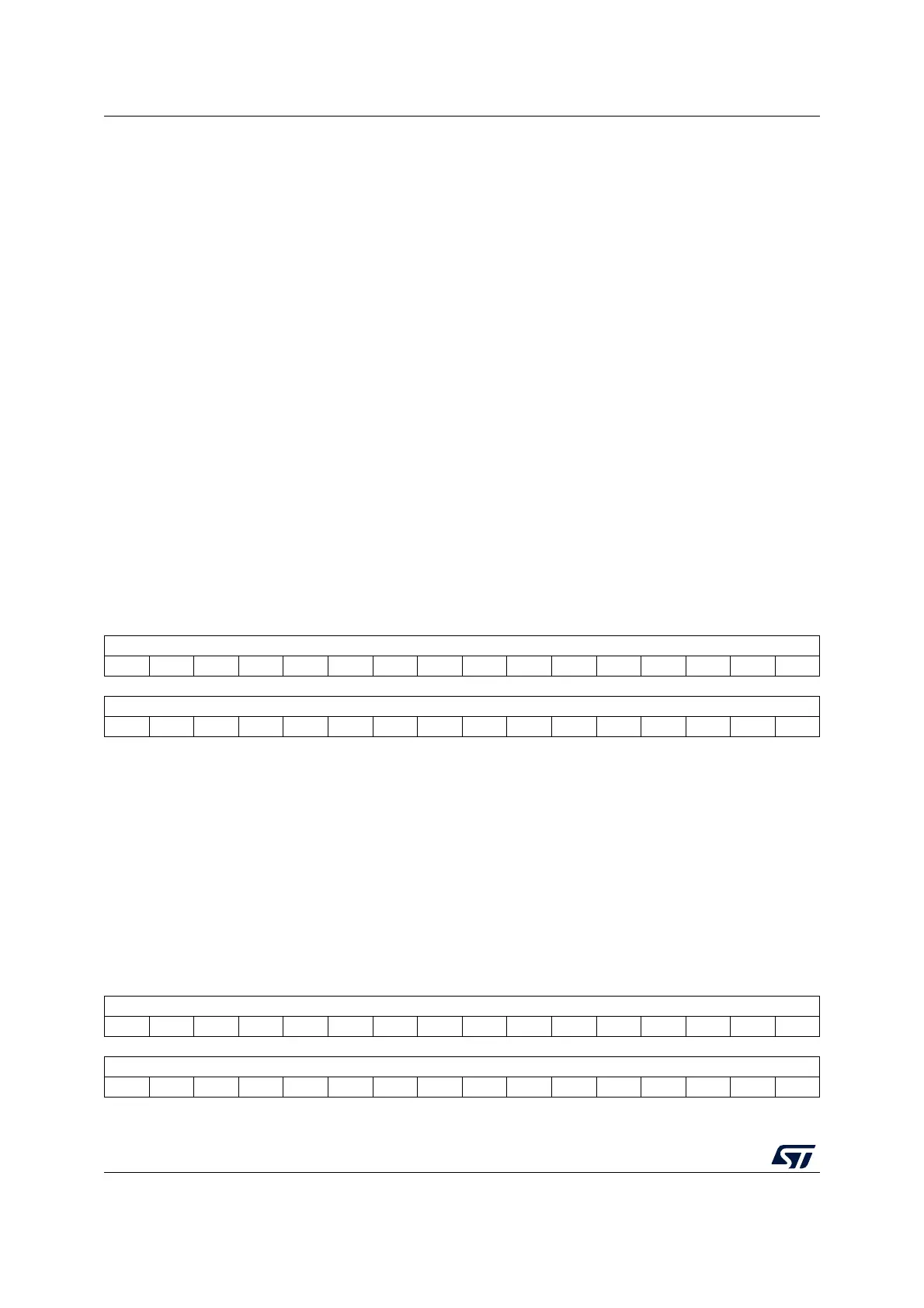
31 30 29 28 27 26 25 24 23 22 21 20 19 18 17 16
KEY[31:16]
wwwwwwwwwwwwwwww
1514131211109876543210
KEY[15:0]
wwwwwwwwwwwwwwww
Bits 31:0 KEY[31:0]: Flash key
The following values must be written consecutively to unlock FLASH_CR and
FLASH_C2CR, thus enabling programming/erasing operations:
KEY1: 0x4567 0123
KEY2: 0xCDEF 89AB
31 30 29 28 27 26 25 24 23 22 21 20 19 18 17 16
OPTKEY[31:16]
wwwwwwwwwwwwwwww
1514131211109876543210
OPTKEY[15:0]
wwwwwwwwwwwwwwww

 Loading...


