Inter-integrated circuit (I2C) interface RM0453
1060/1461 RM0453 Rev 1
This interface can also be connected to a SMBus with the data pin (SDA) and clock pin
(SCL).
If SMBus feature is supported: the additional optional SMBus Alert pin (SMBA) is also
available.
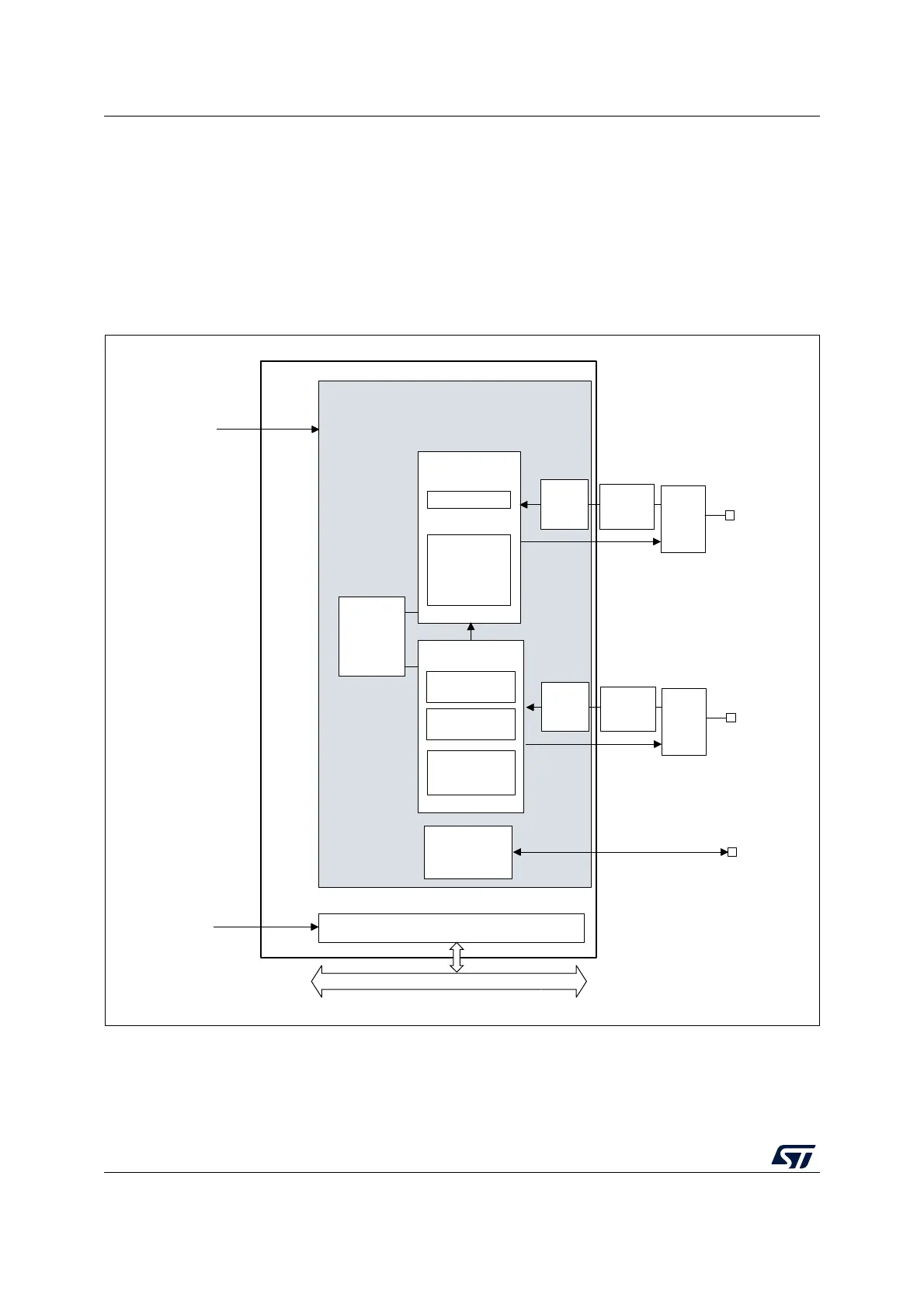
34.4.1 I2C block diagram
The block diagram of the I2C interface is shown in Figure 275.
Figure 275. I2C block diagram
The I2C is clocked by an independent clock source which allows the I2C to operate
independently from the PCLK frequency.
MSv46198V2
I2CCLK
Wakeup
on
address
match
SMBUS
PEC
generation/
check
Shift register
Data control
SMBus
Timeout
check
Clock control
Master clock
generation
Slave clock
stretching
SMBus Alert
control &
status
Digital
noise
filter
I2C_SCL
I2C_SMBA
Registers
APB bus
GPIO
logic
Analog
noise
filter
Digital
noise
filter
I2C_SDA
GPIO
logic
Analog
noise
filter
I2c_pclk
I2c_ker_ck
PCLK

 Loading...


