RM0453 Rev 1 333/1461
RM0453 Reset and clock control (RCC)
364
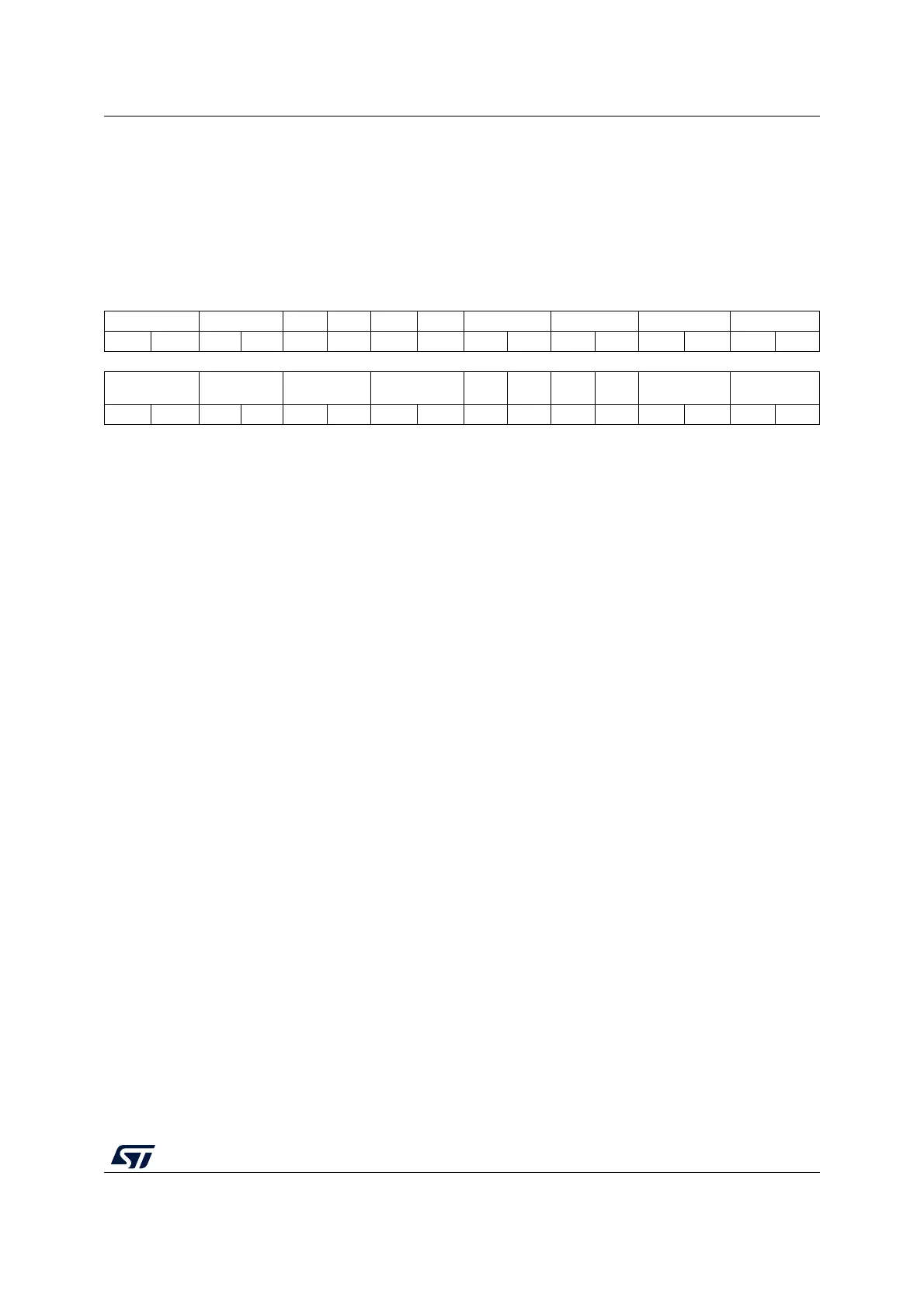
7.4.29 RCC peripherals independent clock configuration register
(RCC_CCIPR)
Address offset: 0x088
Reset value: 0x0000 0000
Access: no wait states, word, half-word and byte access
31 30 29 28 27 26 25 24 23 22 21 20 19 18 17 16
RNGSEL[1:0] ADCSEL[1:0] Res. Res. Res. Res. LPTIM3SEL[1:0] LPTIM2SEL[1:0] LPTIM1SEL[1:0] I2C3SEL[1:0]
rw rw rw rw rw rw rw rw rw rw rw rw
15 14 13 12 11 10 9 8 7 6 5 4 3 2 1 0
I2C2SEL[1:0] I2C1SEL[1:0]
LPUART1SEL
[1:0]
SPI2S2SEL
[1:0]
Res. Res. Res. Res.
USART2SEL
[1:0]
USART1SEL
[1:0]
rw rw rw rw rw rw rw rw rw rw rw rw
Bits 31:30 RNGSEL[1:0]: RNG clock source selection
These bits are set and cleared by software to select the clock source used by the true RNG.
00: PLL “Q” clock (PLLQCLK) selected
01: LSI clock selected
10: LSE clock selected
11: MSI clock selected
Bits 29:28 ADCSEL[1:0]: ADC clock source selection
These bits are set and cleared by software to select the clock source used by the ADC
interface.
00: No clock selected
01: HSI16 clock selected
10: PLL “P” clock (PLLPCLK) selected
11: System clock (SYSCLK) selected
Bits 27:24 Reserved, must be kept at reset value.
Bits 23:22 LPTIM3SEL[1:0]: Low-power timer 3 clock source selection
These bits are set and cleared by software to select the LPTIM3 clock source.
00: PCLK selected
01: LSI clock selected
10: HSI16 clock selected
11: LSE clock selected
Bits 21:20 LPTIM2SEL[1:0]: Low-power timer 2 clock source selection
These bits are set and cleared by software to select the LPTIM2 clock source.
00: PCLK selected
01: LSI clock selected
10: HSI16 clock selected
11: LSE clock selected
Bits 19:18 LPTIM1SEL[1:0]: Low-power timer 1 clock source selection
These bits are set and cleared by software to select the LPTIM1 clock source.
00: PCLK selected
01: LSI clock selected
10: HSI16 clock selected
11: LSE clock selected

 Loading...


