RM0453 Rev 1 645/1461
RM0453 True random number generator (RNG)
649
22.7 RNG registers
The RNG is associated with a control register, a data register and a status register.
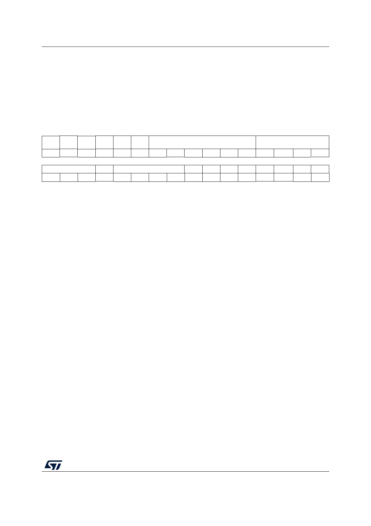
22.7.1 RNG control register (RNG_CR)
Address offset: 0x000
Reset value: 0x0080 0000
31 30 29 28 27 26 25 24 23 22 21 20 19 18 17 16
CONFI
GLOCK
COND
RST
Res. Res. Res. Res. RNG_CONFIG1[5:0] CLKDIV[3:0]
rs rw rw rw rw rw rw rw rw rw rw rw
15 14 13 12 11 10 9 8 7 6 5 4 3 2 1 0
RNG_CONFIG2[2:0] NISTC RNG_CONFIG3[3:0] Res. Res. CED Res. IE RNGEN Res. Res.
rw rw rw rw rw rw rw rw rw rw rw
Bit 31 CONFIGLOCK: RNG Config Lock
0: Writes to the RNG_CR configuration bits [29:4] are allowed.
1: Writes to the RNG_CR configuration bits [29:4] are ignored until the next RNG reset.
This bitfield is set once: if this bit is set it can only be reset to 0 if RNG is reset.
Bit 30 CONDRST: Conditioning soft reset
Write 1 and then write 0 to reset the conditioning logic, clear all the FIFOs and start a new
RNG initialization process, with RNG_SR cleared. Registers RNG_CR and RNG_NSCR are
not changed by CONDRST.
This bit must be set to 1 in the same access that set any configuration bits [29:4]. In other
words, when CONDRST bit is set to 1 correct configuration in bits [29:4] must also be
written.
When CONDRST is set to 0 by software its value goes to 0 when the reset process is done.
It takes about 2 AHB clock cycles + 2 RNG clock cycles.
Bits 29:26 Reserved, must be kept at reset value.
Bits 25:20 RNG_CONFIG1[5:0]: RNG configuration 1
Reserved to the RNG configuration (bitfield 1). Must be initialized using the recommended
value documented in Section 22.6: RNG entropy source validation.
Writing any bit of RNG_CONFIG1 is taken into account only if CONDRST bit is set to 1 in the
same access, while CONFIGLOCK remains at 0. Writing to this bit is ignored if
CONFIGLOCK=1.
Bits 19:16 CLKDIV[3:0]: Clock divider factor
This value used to configure an internal programmable divider (from 1 to 16) acting on the
incoming RNG clock. These bits can be written only when the core is disabled (RNGEN=0).
0x0: internal RNG clock after divider is similar to incoming RNG clock.
0x1: two RNG clock cycles per internal RNG clock.
...
0xF: 2
15
RNG clock cycles per internal clock, e.g. an incoming 48MHz RNG clock becomes
a 1.5 kHz internal RNG clock.
Writing these bits is taken into account only if CONDRST bit is set to 1 in the same access,
while CONFIGLOCK remains at 0. Writing to this bit is ignored if CONFIGLOCK=1.
Bits 15:13 RNG_CONFIG2[2:0]: RNG configuration 2
Reserved to the RNG configuration (bitfield 2). Refer to RNG_CONFIG1 bitfield for details.

 Loading...


