RM0453 Rev 1 819/1461
RM0453 Advanced-control timer (TIM1)
829
25.4.22 TIM1 DMA address for full transfer
(TIM1_DMAR)
Address offset: 0x4C
Reset value: 0x0000 0000
Bits 12:8 DBL[4:0]: DMA burst length
This 5-bit vector defines the length of DMA transfers (the timer recognizes a burst transfer
when a read or a write access is done to the TIMx_DMAR address), i.e. the number of
transfers. Transfers can be in half-words or in bytes (see example below).
00000: 1 transfer
00001: 2 transfers
00010: 3 transfers
...
10001: 18 transfers
Example: Let us consider the following transfer: DBL = 7 bytes & DBA = TIMx_CR1.
– If DBL = 7 bytes and DBA = TIMx_CR1 represents the address of the byte to be
transferred, the address of the transfer should be given by the following equation:
(TIMx_CR1 address) + DBA + (DMA index), where DMA index = DBL
In this example, 7 bytes are added to (TIMx_CR1 address) + DBA, which gives us the
address from/to which the data is copied. In this case, the transfer is done to 7 registers
starting from the following address: (TIMx_CR1 address) + DBA
According to the configuration of the DMA Data Size, several cases may occur:
– If the DMA Data Size is configured in half-words, 16-bit data is transferred to each of the 7
registers.
– If the DMA Data Size is configured in bytes, the data is also transferred to 7 registers: the
first register contains the first MSB byte, the second register, the first LSB byte and so on.
So with the transfer Timer, one also has to specify the size of data transferred by DMA.
Bits 7:5 Reserved, must be kept at reset value.
Bits 4:0 DBA[4:0]: DMA base address
This 5-bits vector defines the base-address for DMA transfers (when read/write access are
done through the TIMx_DMAR address). DBA is defined as an offset starting from the
address of the TIMx_CR1 register.
Example:
00000: TIMx_CR1,
00001: TIMx_CR2,
00010: TIMx_SMCR,
...
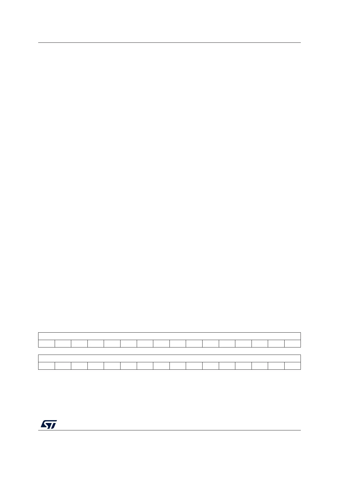
31 30 29 28 27 26 25 24 23 22 21 20 19 18 17 16
DMAB[31:16]
rw rw rw rw rw rw rw rw rw rw rw rw rw rw rw rw
1514131211109876543210
DMAB[15:0]
rw rw rw rw rw rw rw rw rw rw rw rw rw rw rw rw

 Loading...


