RM0453 Rev 1 603/1461
RM0453 Digital-to-analog converter (DAC)
618
Refresh phase:
t
REFRESH
= 7 μs + (2000 * 100 * 10
-9
) * ln(2*10) = 606.1 μs
(where N
LSB
= 10 (10 LSB drop during the hold phase)
Hold phase:
D
v
= i
leak
* t
hold
/ C
SH
= 0.0073 V (10 LSB of 12bit at 3 V)
i
leak
= 150 nA (worst case on the IO leakage on all the temperature range)
t
hold
= 0.0073 * 100 * 10
-9
/ (150 * 10
-9
) = 4.867 ms
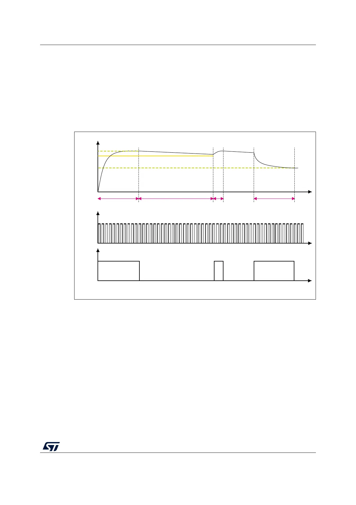
Figure 93. DAC Sample and hold mode phase diagram
Like in Normal mode, the Sample and hold mode has different configurations.
To enable the output buffer, MODE1[2:0] bits in DAC_MCR register must be set to:
• 100: DAC is connected to the external pin
• 101: DAC is connected to external pin and to on chip peripherals
To disabled the output buffer, MODE1[2:0] bits in DAC_MCR register must be set to:
• 110: DAC is connected to external pin and to on chip peripherals
• 111: DAC is connected to on chip peripherals
When MODE1[2:0] bits are equal to 111, an internal capacitor, C
Lint
, holds the voltage
output of the DAC core and then drive it to on-chip peripherals.
All Sample and hold phases are interruptible, and any change in DAC_DHR1 immediately
triggers a new sample phase.
MSv45340V3
dac_hold
_ck
DAC
ON ONON
t
t
V
1
V
2
Sampling phase Hold phase
Refresh
phase
Sampling phase
V
d

 Loading...


