Debug support (DBG) RM0453
1338/1461 RM0453 Rev 1
38.4.5 DP target identification register (DP_TARGETIDR)
Address offset: 0x04
and DP_SELECTR.DPBANKSEL = 2
Reset value: 0x0497 0041
38.4.6 DP data link protocol identification register (DP_DLPIDR)
Address offset: 0x04
and DP_SELECTR.DPBANKSEL = 3
Reset value: 0x0000 0001
Bits 31:10 Reserved, must be kept at reset value.
Bits 9:8 TURNROUND[1:0]: tristate period for SWDIO
0x0: 1 data bit period
0x1: 2 data bit periods
0x2: 3 data bit periods
0x3: 4 data bit periods
Bits 7:0 Reserved, must be kept at reset value.
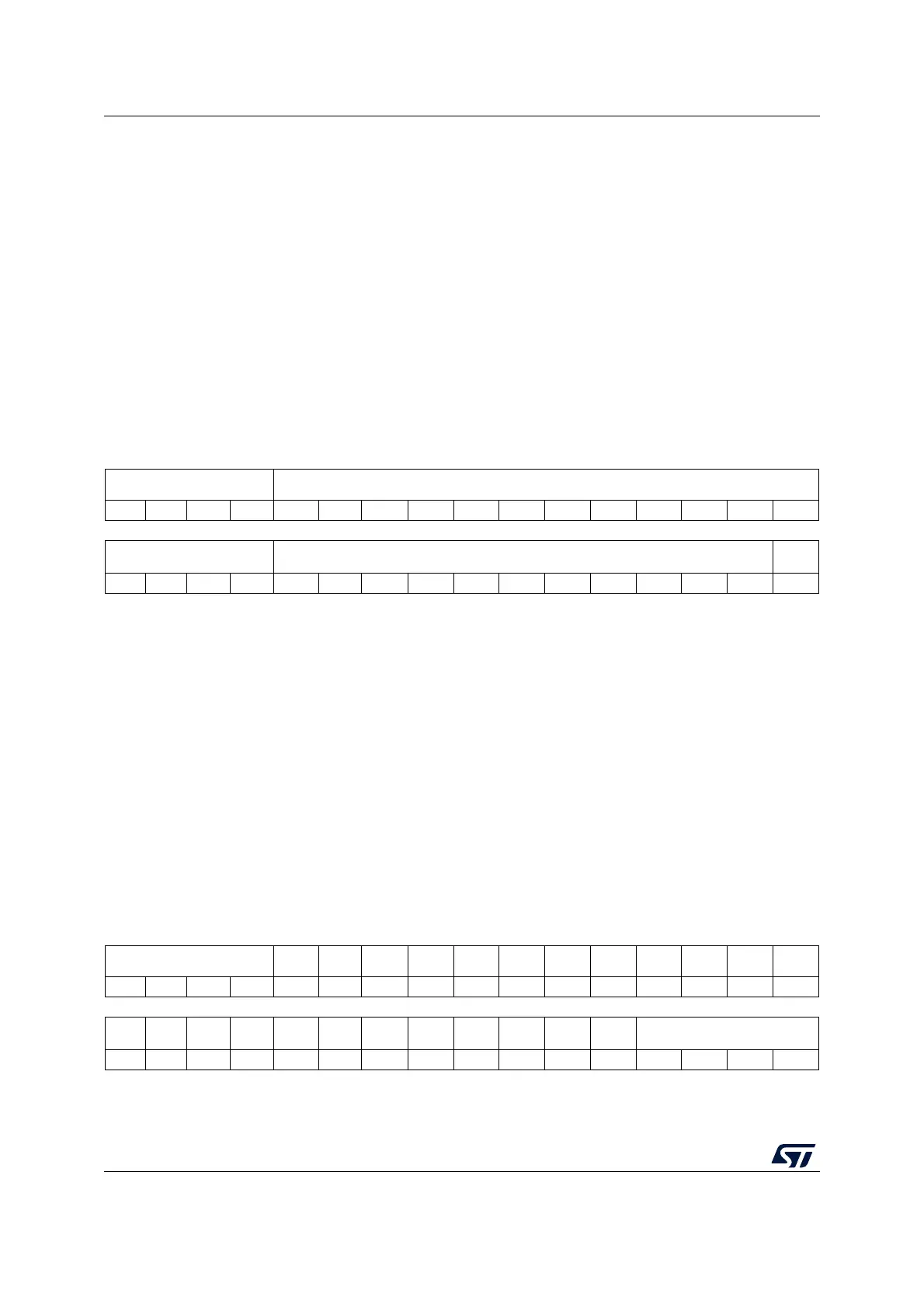
31 30 29 28 27 26 25 24 23 22 21 20 19 18 17 16
TREVISION[3:0] TPARTNO[15:4]
rrrrrrrrrrrrrrrr
15 14 13 12 11 10 9 8 7 6 5 4 3 2 1 0
TPARTNO[3:0] TDESIGNER[10:0] Res.
rrrrrrrrrrrrrrr
Bits 31:28 TREVISION[3:0]: target revision
0x0: revision 1
Bits 27:12 TPARTNO[15:0]: target part number
0x4970: STM32WL5x
Bits 11:1 TDESIGNER[10:0]: target designer JEDEC code.
0x020: STMicroelectronics
Bit 0 Reserved, must be kept at reset value.
31 30 29 28 27 26 25 24 23 22 21 20 19 18 17 16
TINSTANCE[3:0] Res. Res. Res. Res. Res. Res. Res. Res. Res. Res. Res. Res.
rr r r
15 14 13 12 11 10 9 8 7 6 5 4 3 2 1 0
Res. Res. Res. Res. Res. Res. Res. Res. Res. Res. Res. Res. PROTSVN[3:0]
rrrr

 Loading...


