RM0453 Rev 1 395/1461
RM0453 General-purpose I/Os (GPIO)
427
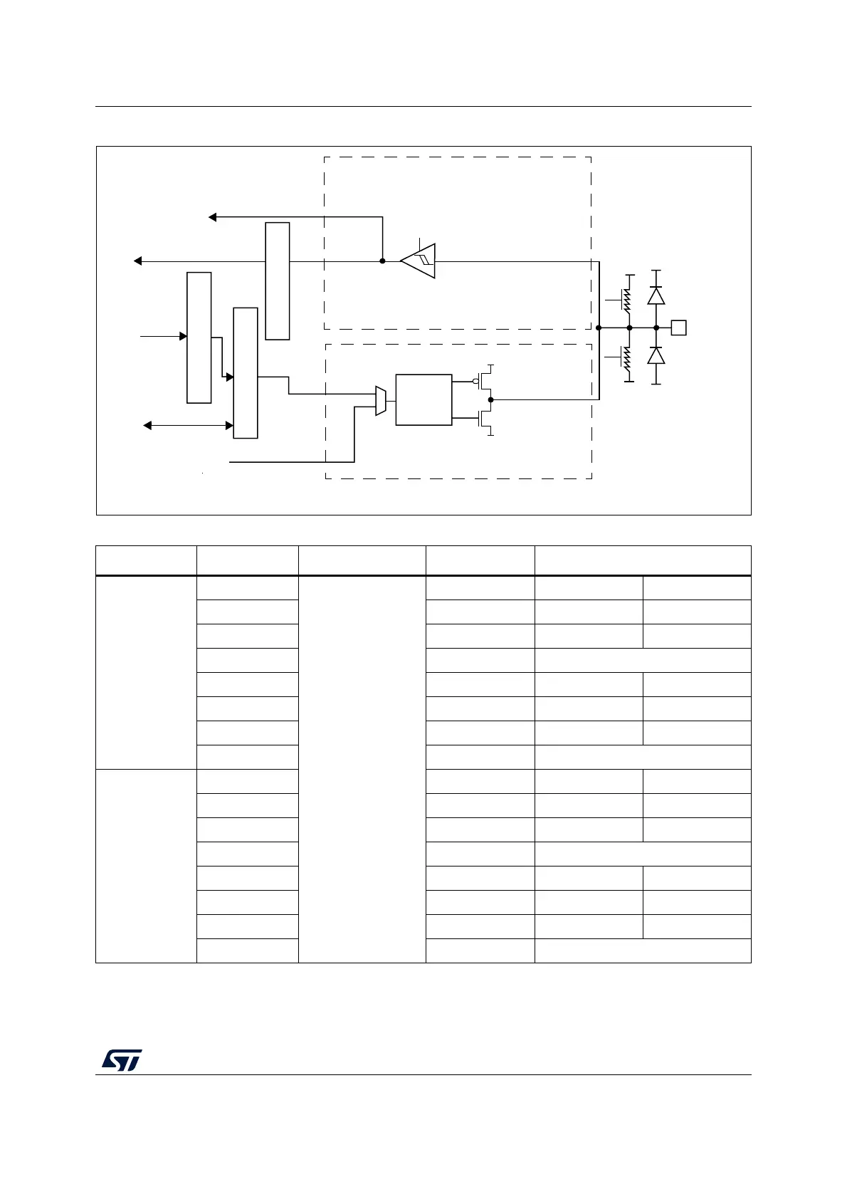
Figure 44. Basic structure of a 5V-tolerant I/O port bit
Alternate function output
Alternate function input
Push-pull,
open-drain or
disabled
Output data register
Read/write
From on-chip
peripheral
To on-chip
peripheral
Output
control
on/off
Pull
Pull
on/off
I/O pin
V
DDIOx
V
DDIOx
V
SS
V
SS
TTL Schmitt
trigger
V
SS
V
DD_FT
(1)
Protection
diode
Protection
diode
on/off
Input driver
Output driver
down
up
P-MOS
N-MOS
Read
Bit set/reset registers
Write
Input data register
ai15939e
1) VDD_FT is specific to 5V-tolerant I/Os and different from VDD.
Table 70. Port bit configurations
MODE(i)[1:0] OTYPER(i) OSPEED(i)[1:0] PUPD(i)[1:0] I/O configuration
(1)
01
0
SPEED[1:0]
00 GP output PP
0 01 GP output PP + PU
0 10 GP output PP + PD
0 11 Reserved
1 00 GP output OD
1 01 GP output OD + PU
1 10 GP output OD + PD
1 11 Reserved (GP output OD)
10
000AFPP
001AFPP + PU
010AFPP + PD
0 11 Reserved
100AFOD
101AFOD + PU
110AFOD + PD
1 11 Reserved

 Loading...


