RM0453 Rev 1 849/1461
RM0453 General-purpose timer (TIM2)
901
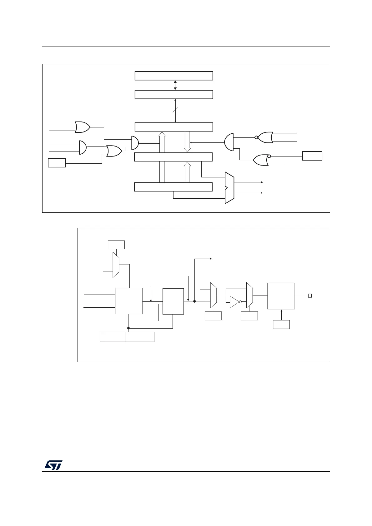
Figure 214. Capture/Compare channel 1 main circuit
Figure 215. Output stage of Capture/Compare channel (channel 1)
The capture/compare block is made of one preload register and one shadow register. Write
and read always access the preload register.
In capture mode, captures are actually done in the shadow register, which is copied into the
preload register.
In compare mode, the content of the preload register is copied into the shadow register
which is compared to the counter.
MSv63030V1
CC1E
compare shadow register
Comparator
Capture/compare preload register
Counter
IC1PS
CC1S[0]
CC1S[1]
Capture
Input mode
CC1S[0]
CC1S[1]
Output mode
UEV
OC1PE
(from time
base unit)
Compare
transfer
APB Bus
16/32-bit
MCU-peripheral interface
TIMx_CCMR1
OC1PE
CNT>CCR1
CNT=CCR1
TIMx_EGR
CC1G
MS33145V5
Output
mode
controller
CNT > CCR1
CNT = CCR1
TIMx_CCMR1
OC1M[3:0]
0
1
CC1P
TIMx_CCER
Output
enable
circuit
OC1
CC1E
TIMx_CCER
To the master
mode controller
OC1REF
OC1CE
0
1
CC1E
TIMx_CCER
‘0’
0
1
ocref_clr_int
ETRF
OCREF_CLR
OCCS
TIMx_SMCR
Output
selector
OC2REF
OC1REFC

 Loading...


