RM0453 Rev 1 535/1461
RM0453 Analog-to-digital converter (ADC)
592
18.3.2 ADC voltage regulator (ADVREGEN)
The ADC has a specific internal voltage regulator which must be enabled and stable before
using the ADC.
The ADC internal voltage regulator can be enabled by setting ADVREGEN bit to 1 in the
ADC_CR register. The software must wait for the ADC voltage regulator startup time
(t
ADCVREG_SETUP
) before launching a calibration or enabling the ADC. This delay must be
managed by software (for details on t
ADCVREG_SETUP
, refer to the device datasheet).
After ADC operations are complete, the ADC is disabled (ADEN = 0). It is then possible to
save additional power by disabling the ADC voltage regulator (refer to Section : ADC
voltage regulator disable sequence).
Note: When the internal voltage regulator is disabled, the internal analog calibration is kept.
Analog reference from the power control unit
The internal ADC voltage regulator internally uses an analog reference delivered by the
power control unit through a buffer. This buffer is always enabled when the main voltage
regulator of the power control unit operates in normal Run mode (refer to Reset and clock
control and power control sections).
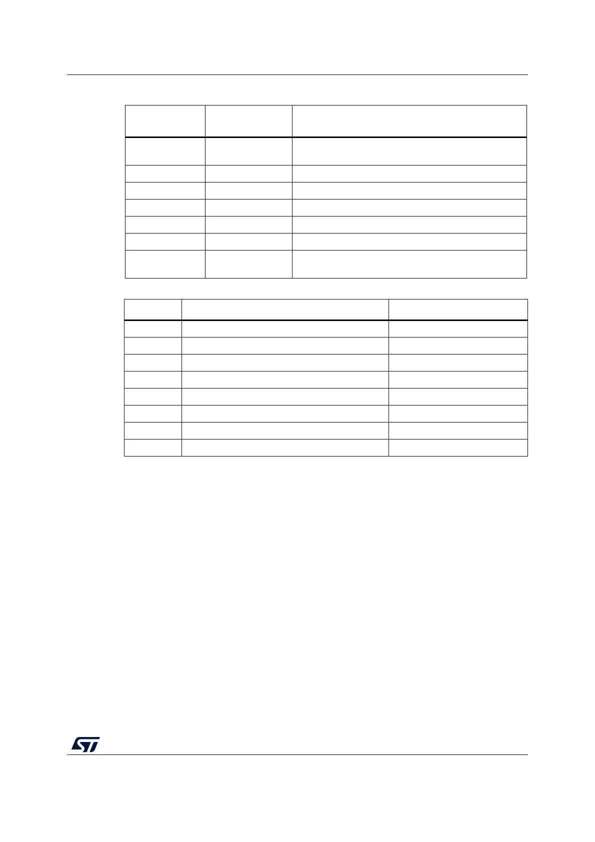
Table 101. ADC internal input/output signals
Internal signal
name
Signal type Description
V
IN
[x]
Analog Input
channels
Connected either to internal channels or to ADC_INi
external channels
TRGx Input ADC conversion triggers
V
TS
Input Internal temperature sensor output voltage
V
REFINT
Input Internal voltage reference output voltage
V
BAT/3
Input VBAT pin input voltage divided by 3
dac_out1 Input DAC internal channel1 input
ADC_AWDx_OUT Output
Internal analog watchdog output signal connected to on-
chip timers (x = Analog watchdog number = 1,2,3)
Table 102. External triggers
Name Source EXTSEL[2:0]
TRG0 TIM1_TRGO2 000
TRG1 TIM1_CC4 001
TRG2 TIM2_TRGO 010
TRG3 TIM2_CH4 011
TRG4 Reserved 100
TRG5 TIM2_CH3 101
TRG6 Reserved 110
TRG7 EXTI11 111

 Loading...


