Debug support (DBG) RM0453
1340/1461 RM0453 Rev 1
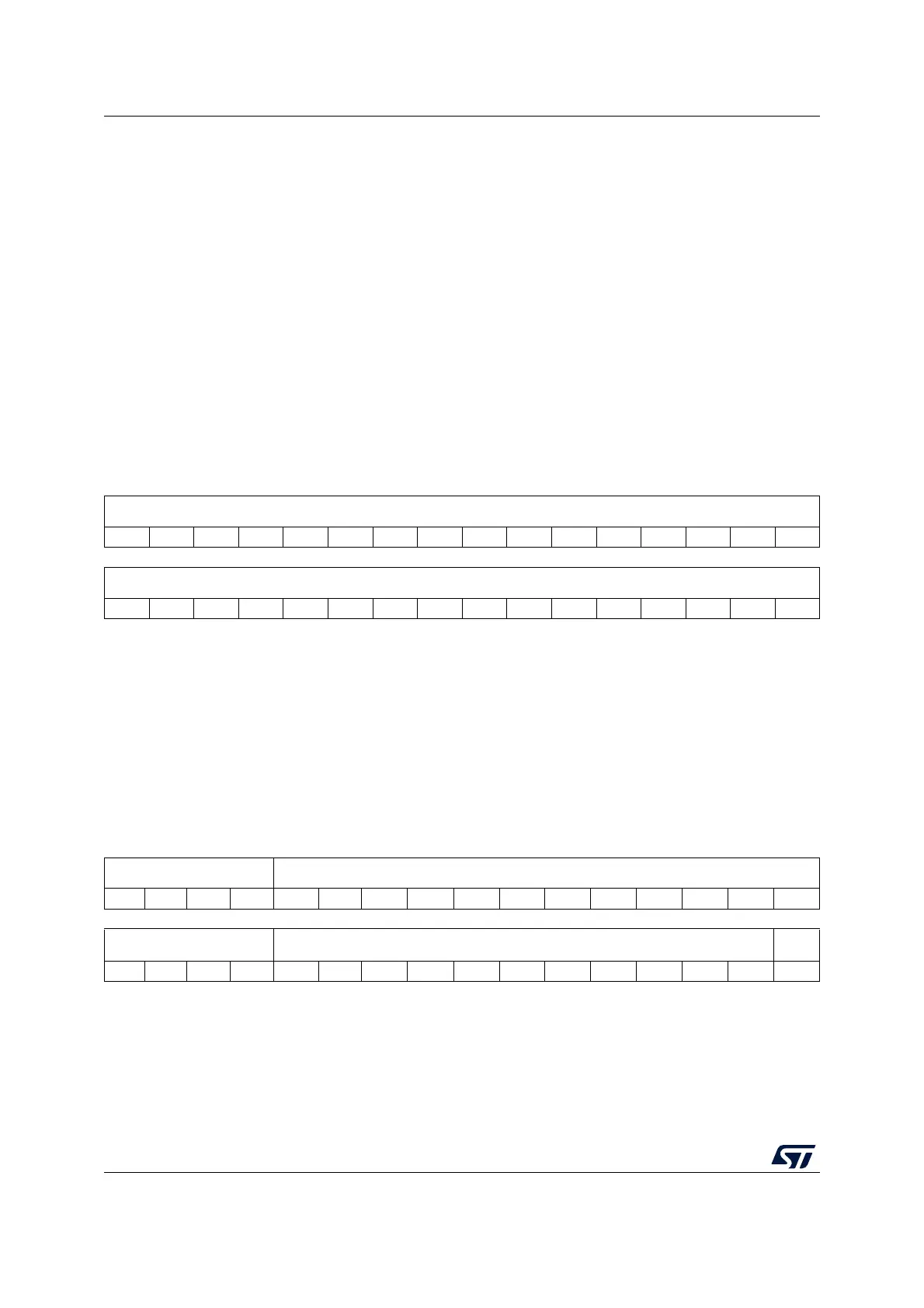
38.4.9 DP read buffer register (DP_BUFFR)
Address offset: 0x0C
Reset value: 0x0000 0000
38.4.10 DP target identification register (DP_TARGETSELR)
Address offset: 0x0C
Reset value: 0xXXXX XXXX
Bits 27:8 Reserved, must be kept at reset value.
Bits 7:4 APBANKSEL[3:0]: AP register bank selection
Selects the 4-word register bank on the active AP for the next transaction.
Bits 3:0 DPBANKSEL[3:0]: DP register bank selection
Selects the register at address 0x4 of the debug port.
0x0: DP_CTRLSTATR
0x1: DP_DLCR
0x2: DP_TARGETIDR
0x3: DP_DLPIDR
0x4 to 0xF: reserved
31 30 29 28 27 26 25 24 23 22 21 20 19 18 17 16
RDBUFF[31:16]
rrrrrrrrrrrrrrrr
1514131211109876543210
RDBUFF[15:0]
rrrrrrrrrrrrrrrr
Bits 31:0 RDBUFF[31:0]: Contains the value returned by the last AP read access.
The value returned by an AP read access can either be obtained using a second read access
to the same address, which initiates a new transaction on the corresponding bus, or else it
can be read from this register, in which case no new AP transaction occurs.
31 30 29 28 27 26 25 24 23 22 21 20 19 18 17 16
TINSTANCE[3:0] TPARTNO[15:4]
wwwwwwwwwwwwwwww
1514131211109876543210
TPARTNO[3:0] TDESIGNER[10:0] Res.
wwwwwwwwwwwwwww

 Loading...


