RM0453 Rev 1 595/1461
RM0453 Digital-to-analog converter (DAC)
618
19.4 DAC functional description
19.4.1 DAC block diagram
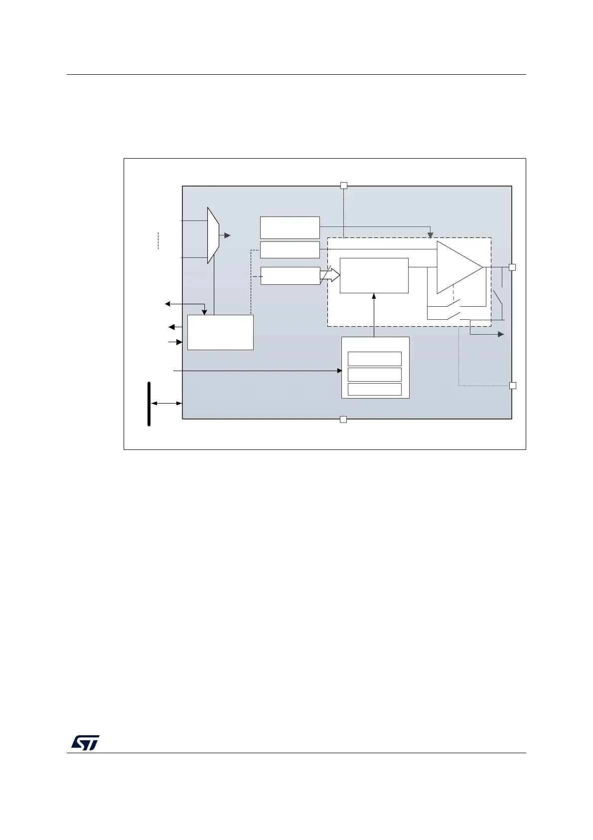
Figure 86. DAC block diagram
1. MODE1 bits in the DAC_MCR control the output mode and allow switching between the Normal mode in
buffer/unbuffered configuration and the Sample and hold mode.
19.4.2 DAC pins and internal signals
The DAC includes:
• One output channel
• The DACx_OUT1 can be disconnected from the output pin and used as an ordinary
GPIO
• The dac_out1 can use an internal pin connection to on-chip peripherals such as
comparator, operational amplifier and ADC (if available).
• DAC output channel buffered or non buffered
• Sample and hold block and registers operational in Stop mode, using the LSI clock
source (dac_hold_ck) for static conversion.
The DAC includes up to two separate output channels. Each output channel can be
connected to on-chip peripherals such as comparator, operational amplifier and ADC (if
available). In this case, the DAC output channel can be disconnected from the DACx_OUT1
output pin and the corresponding GPIO can be used for another purpose.
The DAC output can be buffered or not. The Sample and hold block and its associated
registers can run in Stop mode using the LSI clock source (dac_hold_ck).
MSv61355V5
V
REF+
dac_out1
DAC_OUT1
Buffer
TSAMPLE1
THOLD1
TREFRESH1
Sample and hold
registers
TSEL1
[3:0]
bits
TRIG
dac_ch1_dma
dac_ch1_trg1
dac_ch1_trg15
32-bit APB
bus
DAC
converter
DOR1
Offset
calibration
OTRIM1[5:0]
bits
12-bit
MODE1 bits
dac_unr_it
dac_pclk
V
DD
V
SS
dac_hold_ck
Control registers
and logic
channel1

 Loading...


