Memory and bus architecture RM0453
62/1461 RM0453 Rev 1
SRAM2, the AHB1 peripherals including the APB1 and APB2 peripherals, the AHB2
peripherals and the AHB3 peripherals including the APB3 peripherals.
2.1.5 S4, S5: DMA-bus
These buses connect the AHB master interface of the DMAs to the bus matrix.The targets of
this bus are the internal Flash memory, SRAM1, SRAM2 the AHB1 peripherals including the
APB1 and APB2 peripherals, the AHB2 peripherals and the AHB3 peripherals including the
APB3 peripherals.
AHB/APB bridges
The two bridges AHB to APB1 and AHB to ABP2 provide full synchronous connections
between the AHB1 and the two APB buses, allowing flexible selection of the peripheral
frequency.
The bridge AHB to APB3 provides full synchronous connections between the AHB and the
APB bus, allowing flexible selection of the frequency between the AHB and peripherals.
Refer to Section 2.6.2: Memory map and register boundary addresses for the address
mapping of the peripherals connected to this bridge.
After each device reset, all peripheral clocks are disabled, except for the SRAM1/2 and the
Flash memory interface. Before using a peripheral, its clock must be enabled in the
RCC_AHBxENR and RCC_APBxENR registers.
Note: When a 16- or 8-bit access is performed on an APB register, the access is transformed into
a 32-bit access: the bridge duplicates the 16- or 8-bit data to feed the 32-bit vector.
2.2 Boot configuration
Three different CPU1 boot modes and one CPU2 boot mode can be selected through the
BOOT0 pin and nBOOT1 bit in the user options.
Boot is furthermore conditioned by the CPU1 boot lock enable, CPU2 boot lock enable and
the user Flash memory empty check, as shown in the table below.
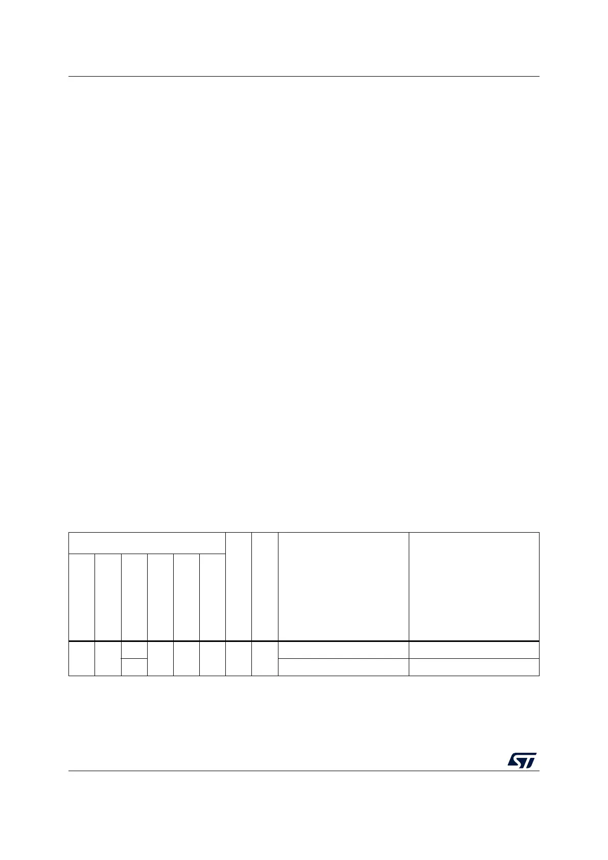
Table 1. Device boot mode
Boot mode selection
Valid options
User Flash empty
CPU1 aliasing space CPU2 boot
nBOOT1 option
nBOOT0 option
PH3/BOOT0
nSWBOOT0
option
BOOT_LOCK
C2BOOT_LOCK
xx
0
XxxNox
Hold SFI/RSS boot
(1)(2)(3)
1 SRAM1 boot Hold

 Loading...


