General-purpose timers (TIM16/TIM17) RM0453
940/1461 RM0453 Rev 1
Note: The state of the external I/O pins connected to the complementary OCx and OCxN channels
depends on the OCx and OCxN channel state
and AFIO registers.
27.4.9 TIMx counter (TIMx_CNT)(x = 16 to 17)
Address offset: 0x24
Reset value: 0x0000 0000
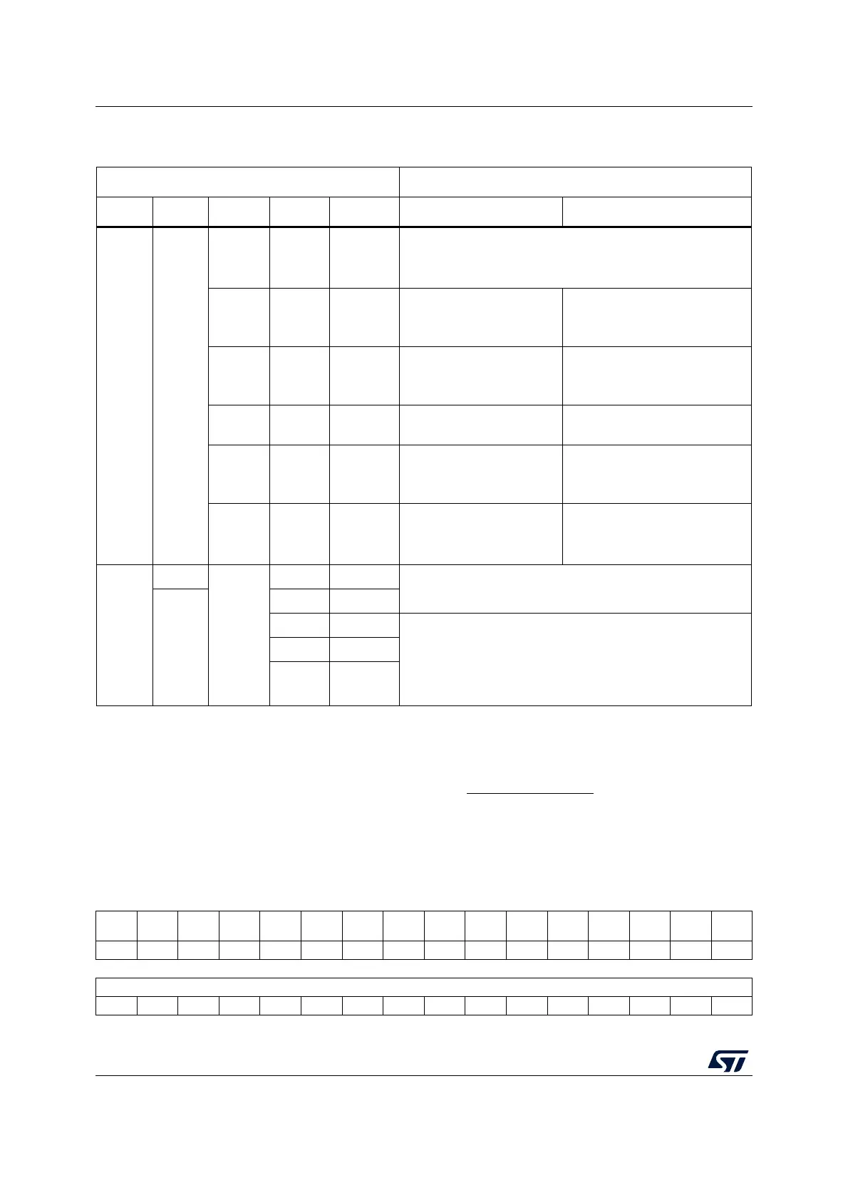
Table 187. Output control bits for complementary OCx and OCxN channels with break feature
(TIM16/17)
Control bits Output states
(1)
MOE bit OSSI bit OSSR bit CCxE bit CCxNE bit OCx output state OCxN output state
1X
X0 0
Output Disabled (not driven by the timer: Hi-Z)
OCx=0
OCxN=0, OCxN_EN=0
00 1
Output Disabled (not driven
by the timer: Hi-Z)
OCx=0
OCxREF + Polarity
OCxN=OCxREF XOR CCxNP
01 0
OCxREF + Polarity
OCx=OCxREF XOR CCxP
Output Disabled (not driven by
the timer: Hi-Z)
OCxN=0
X1 1
OCREF + Polarity + dead-
time
Complementary to OCREF (not
OCREF) + Polarity + dead-time
10 1
Off-State (output enabled
with inactive state)
OCx=CCxP
OCxREF + Polarity
OCxN=OCxREF XOR CCxNP
11 0
OCxREF + Polarity
OCx=OCxREF XOR CCxP,
OCx_EN=1
Off-State (output enabled with
inactive state)
OCxN=CCxNP, OCxN_EN=1
0
0
X
XX
Output disabled (not driven by the timer: Hi-Z).
1
00
0 1 Off-State (output enabled with inactive state)
Asynchronously: OCx=CCxP, OCxN=CCxNP
Then if the clock is present: OCx=OISx and OCxN=OISxN
after a dead-time, assuming that OISx and OISxN do not
correspond to OCX and OCxN both in active state
10
11
1. When both outputs of a channel are not used (control taken over by GPIO controller), the OISx, OISxN, CCxP and CCxNP
bits must be kept cleared.
31 30 29 28 27 26 25 24 23 22 21 20 19 18 17 16
UIF
CPY
Res. Res. Res. Res. Res. Res. Res. Res. Res. Res. Res. Res. Res. Res. Res.
r
1514131211109876543210
CNT[15:0]
rw rw rw rw rw rw rw rw rw rw rw rw rw rw rw rw

 Loading...


