AES hardware accelerator (AES) RM0453
684/1461 RM0453 Rev 1
DMA transfer must not include the last block. For details, refer to Section 23.4.4: AES
procedure to perform a cipher operation.
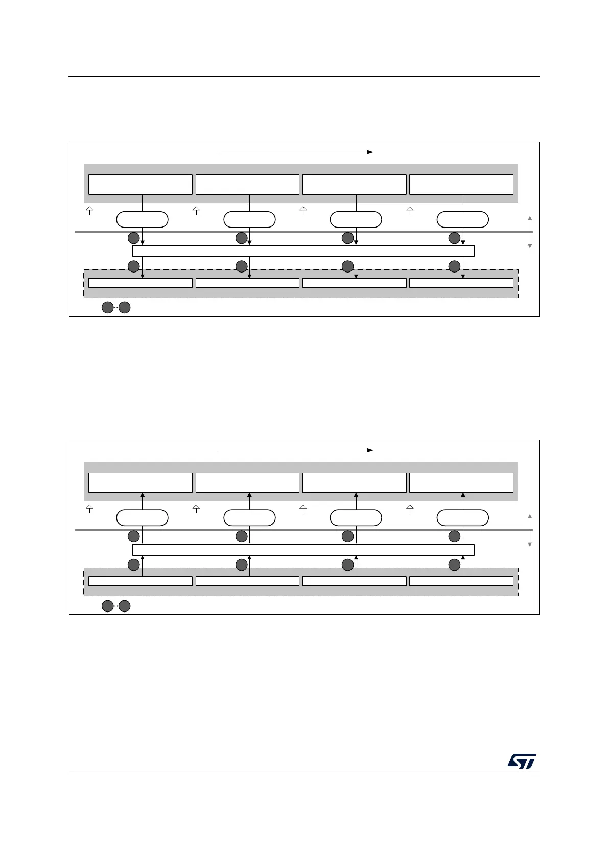
Figure 125. DMA transfer of a 128-bit data block during input phase
Data output using DMA
Setting the DMAOUTEN bit of the AES_CR register enables DMA reading from AES. The
AES peripheral then initiates a DMA request during the Output phase each time it requires
to read a 128-bit block (quadruple word) to the AES_DINR register, as shown in Figure 126.
Note: According to the message size, extra bytes might need to be discarded by application in the
last block.
Figure 126. DMA transfer of a 128-bit data block during output phase
DMA operation in different operating modes
DMA operations are usable when Mode 1 (encryption) or Mode 3 (decryption) are selected
via the MODE[1:0] bitfield of the register AES_CR. As in Mode 2 (key derivation) the
AES_KEYRx registers must be written by software, enabling the DMA transfer through the
DMAINEN and DMAOUTEN bits of the AES_CR register have no effect in that mode.
DMA single requests are generated by AES until it is disabled. So, after the data output
phase at the end of processing of a 128-bit data block, AES switches automatically to a new
data input phase for the next data block, if any.
MSv42160V1
AES core input buffer
AES_DINR
LSB
MSB
(No swapping)
Memory accessed through DMA
Word2Word3 Word0Word1
DMA
single write
DMA req N DMA req N+1 DMA req N+2 DMA req N+3
I127 I96
I63 I32
I31 I0
I64I95
D127 D96
D63 D32
D31 D0
D64D95
DIN[127:96] DIN[95:64] DIN[63:32] DIN[31:0]
DMA
single write
DMA
single write
DMA
single write
Chronological order
Increasing address
LSBMSB
AES
peripheral
System
1 2 3 4
1
Order of write to AES_DINR
1 2 3 4
4
MSv42161V1
AES core output buffer
LSB
MSB
(No swapping)
Memory accessed through DMA
Word2Word3 Word0Word1
DMA
single read
DMA req N DMA req N+1 DMA req N+2 DMA req N+3
O127 O96
O63 O32
O31 O0
O64O95
D127 D96
D63 D32
D31 D0
D64D95
DOUT[127:96] DOUT[95:64] DOUT[63:32] DOUT[31:0]
DMA
single read
DMA
single read
DMA
single read
Chronological order
Increasing address
LSBMSB
System
AES
peripheral
1 2 3 4
1 2 3 4
1
Order of read from AES_DOUTR
4
AES_DOUTR

 Loading...


