RM0453 Rev 1 1329/1461
RM0453 Debug support (DBG)
1448
one associated with an instruction register (IR) and the other one with a number of data
registers (DR).
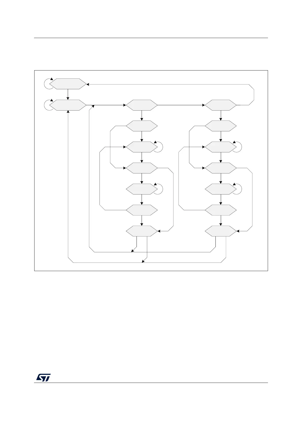
Figure 384. JTAG TAP state machine
The operation of the JTAG-DP is as follows:
• When the TAPSM goes through the Capture-IR state, 0b0001 is transferred onto the
instruction register (IR) scan chain. The IR scan chain is connected between JTDI and
JTDO.
• While the TAPSM is in the Shift-IR state, the IR scan chain shifts one bit for each rising
edge of JTCK. This means that, on the first tick:
– The LSB of the IR scan chain is output on JTDO.
– Bit[n] of the IR scan chain is transferred to bit[n-1].
– The value on JTDI is transferred to the MSB of the IR scan chain.
• When the TAPSM goes through the Update-IR state, the value scanned into the IR
scan chain is transferred into the instruction register.
• When the TAPSM goes through the Capture-DR state, a value is transferred from one
of the data registers onto one of the DR scan chains, connected between JTDI and
MSv60366V1
Test-Logic-
Reset
Run-Test/
Idle
Select-
DR-Scan
Shift-DR
Capture-
DR
Exit1-DR
Pause-
DR
Exit2-DR
Update-
DR
Select-
IR-Scan
Shift-IR
Capture-
IR
Exit1-IR
Pause-IR
Exit2-IR
Update-
IR
JTMS=0
JTMS=1
JTMS=1
JTMS=0
JTMS=1
JTMS=0
JTMS=1
JTMS=1
JTMS=0
JTMS=0
JTMS=0
JTMS=1 JTMS=0 JTMS=0JTMS=1
JTMS=0
JTMS=1
JTMS=1
JTMS=0
JTMS=0
JTMS=1
JTMS=1 JTMS=0
JTMS=0
JTMS=1
JTMS=1
JTMS=0
JTMS=0
JTMS=1
JTMS=1 JTMS=0
JTMS=1

 Loading...


