RM0453 Rev 1 351/1461
RM0453 Reset and clock control (RCC)
364
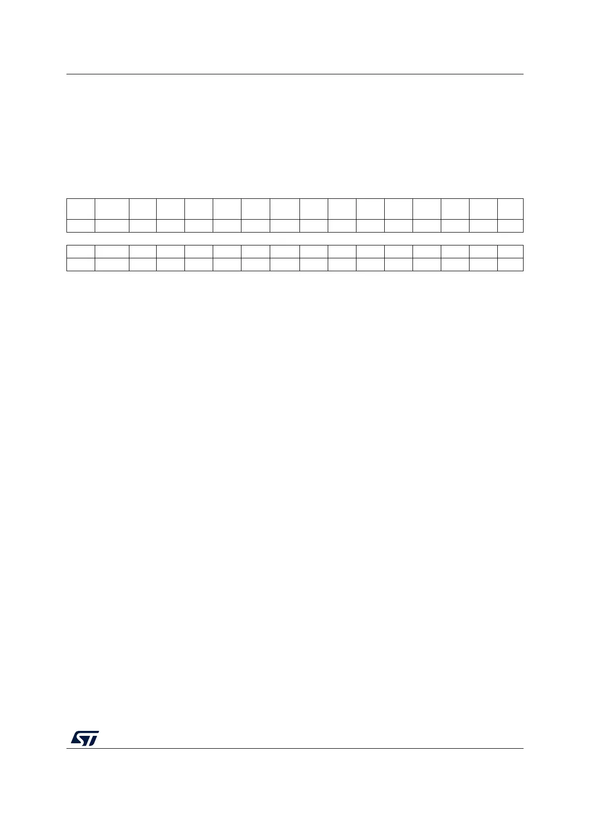
7.4.42 RCC CPU2 AHB3 peripheral clock enable in Sleep mode register
(RCC_C2AHB3SMENR)
Address offset: 0x170
Reset value: 0x0387 0000
Access: no wait state, word, half-word and byte access
31 30 29 28 27 26 25 24 23 22 21 20 19 18 17 16
Res. Res. Res. Res. Res. Res.
FLASH
SMEN
SRAM2
SMEN
SRAM1
SMEN
Res. Res. Res. Res.
RNG
SMEN
AES
SMEN
PKA
SMEN
rw rw rw rw rw rw
1514131211109 8 76543210
Res. Res. Res. Res. Res. Res. Res. Res. Res. Res. Res. Res. Res. Res. Res. Res.
Bits 31:26 Reserved, must be kept at reset value.
Bit 25 FLASHSMEN: Flash memory interface clock enable during CPU2 CSleep and CStop modes
This bit is set and cleared by software.
0: Flash memory interface clock disabled by the clock gating during CPU2 CSleep and
CStop modes
1: Flash memory interface clock enabled by the clock gating during CPU2 CSleep mode,
disabled during CPU2 CStop mode.
Bit 24 SRAM2SMEN: SRAM2 interface clock enable during CPU2 CSleep and CStop modes
This bit is set and cleared by software.
0: SRAM2 clock disabled by the clock gating during CPU2 CSleep and CStop modes
1: SRAM2 clock enabled by the clock gating during CPU2 CSleep mode, disabled during
CPU2 CStop mode
Bit 23 SRAM1SMEN: SRAM1 interface clock enable during CPU2 CSleep and CStop modes
This bit is set and cleared by software.
0: SRAM1 interface clock disabled by the clock gating during CPU2 CSleep and CStop
modes
1: SRAM1 interface clock enabled by the clock gating during CPU2 CSleep mode, disabled
during CPU2 CStop mode
Bits 22:19 Reserved, must be kept at reset value.
Bit 18 RNGSMEN: True RNG clock enable during CPU2 CSleep and CSleep and CStop modes
This bit is set and cleared by software.
0: True RNG bus clock disabled by the clock gating during CPU2 CSleep and CStop modes
1: True RNG bus clock enabled by the clock gating during CPU2 CSleep mode, disabled
during CPU2 CStop mode

 Loading...


