Analog-to-digital converter (ADC) RM0453
584/1461 RM0453 Rev 1
18.12.9 ADC channel selection register [alternate] (ADC_CHSELR)
Address offset: 0x28
Reset value: 0x0000 0000
The same register can be used in two different modes:
– Each ADC_CHSELR bit enables an input (CHSELRMOD = 0 in ADC_CFGR1). Refer to the current
section.
– ADC_CHSELR is able to sequence up to 8 channels (CHSELRMOD = 1 in ADC_CFGR1). Refer to
next section.
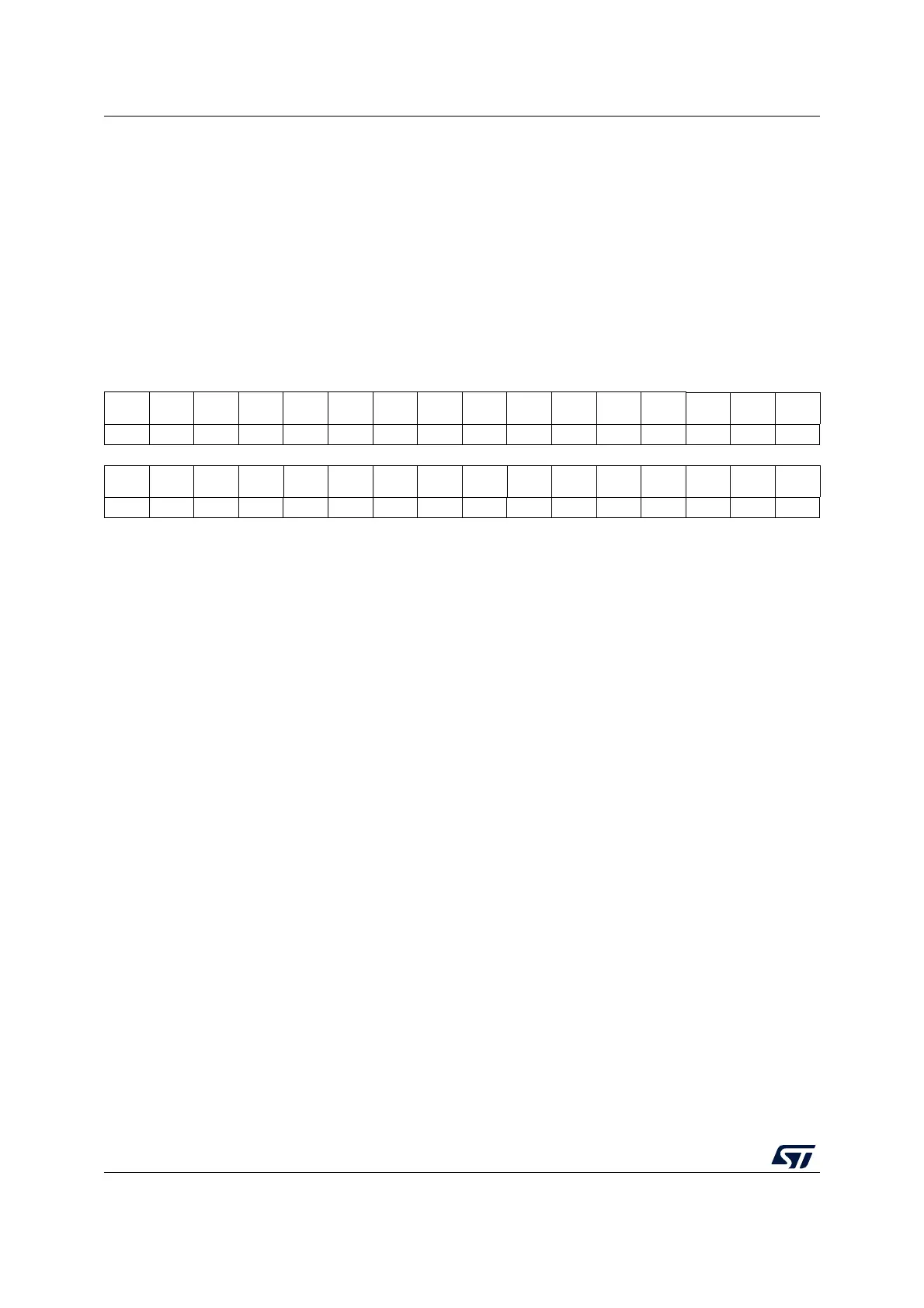
CHSELRMOD = 0 in ADC_CFGR1:
31 30 29 28 27 26 25 24 23 22 21 20 19 18 17 16
Res. Res. Res. Res. Res. Res. Res. Res. Res. Res. Res. Res. Res. Res.
CHSEL
17
CHSEL
16
rw rw
1514131211109876543210
CHSEL
15
CHSEL
14
CHSEL
13
CHSEL
12
CHSEL
11
CHSEL
10
CHSEL
9
CHSEL
8
CHSEL
7
CHSEL
6
CHSEL
5
CHSEL
4
CHSEL
3
CHSEL
2
CHSEL
1
CHSEL
0
rw rw rw rw rw rw rw rw rw rw rw rw rw rw rw rw
Bits 31:18 Reserved, must be kept at reset value.
Bits 17:0 CHSEL[17:0]: Channel-x selection
These bits are written by software and define which channels are part of the sequence of channels to
be converted.
0: Input Channel-x is not selected for conversion
1: Input Channel-x is selected for conversion
Note: The software is allowed to write this bit only when ADSTART = 0 (which ensures that no
conversion is ongoing).
If CCRDY is not yet asserted after channel configuration (writing ADC_CHSELR register or
changing CHSELRMOD or SCANDIR), the value written to this bit is ignored.

 Loading...


