RM0453 Rev 1 1343/1461
RM0453 Debug support (DBG)
1448
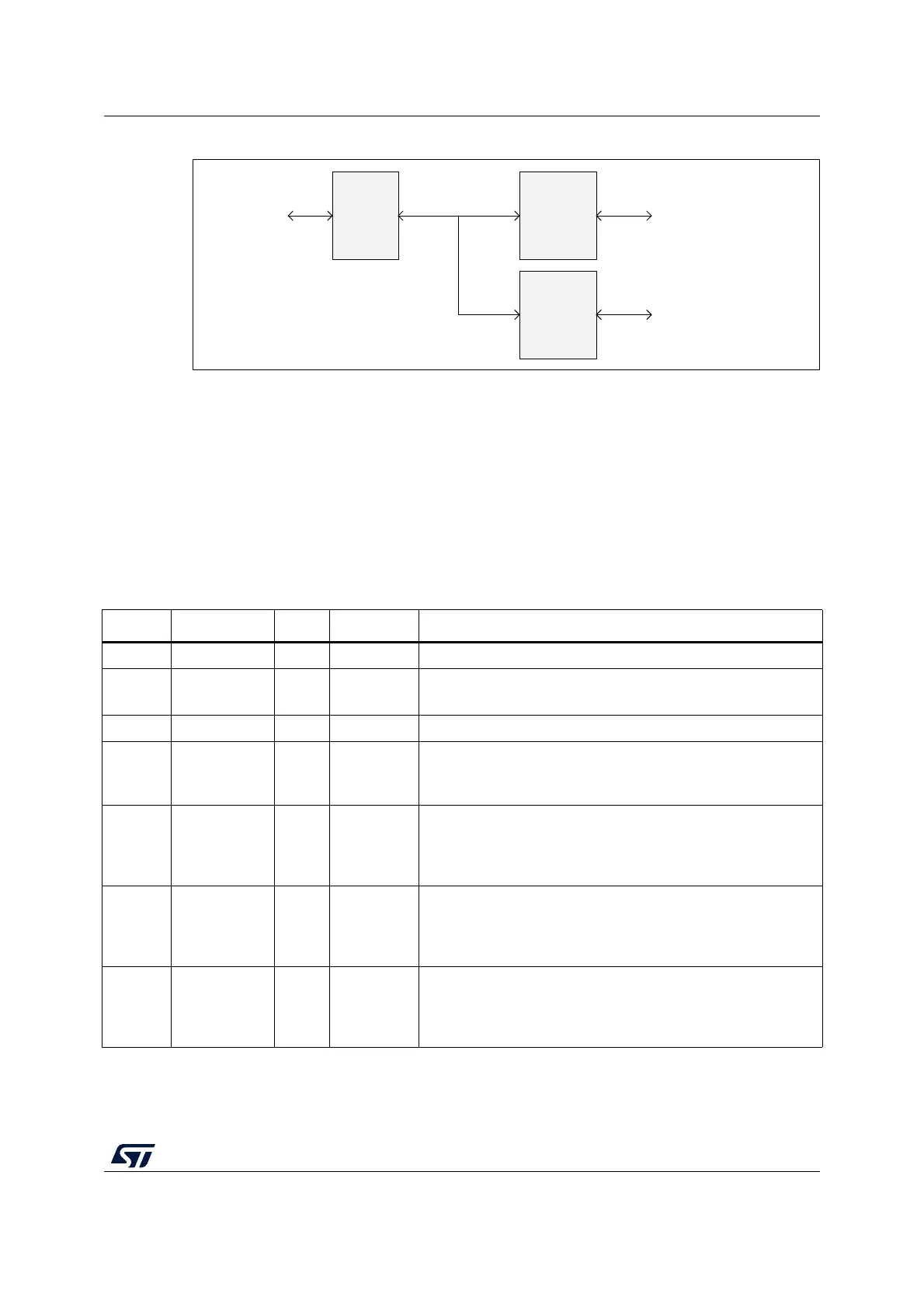
Figure 385. Debug and access port connections
The address of the AP registers is composed as follows:
• Bits [7:4]: content of the APBANKSEL[3:0] field in the DP_SELECTR register
(see Section 38.4.8)
• Bits [3:2]: content of the A(3:2) field of the APACC data register in the JTAG-DP
(see Table 268: DP register map and reset values) or of the SW-DP packet request
(see Table 264: Packet request), depending on the debug interface used
• Bits [1:0]: always set to 0
The content of the APSEL[3:0] field of the DP_SELECTR register defines which MEM-AP is
being accessed.
MSv60367V1
SWJ-DP
AP0
(AHB-AP)
AP1
(AHB-AP)
DAPBUS
JTAG/SWD CPU1 Cortex-M4
CPU2 Cortex-M0+
Table 269. MEM-AP registers
Address APBANKSEL A(3:2) Name Description
0x00 0x0 0 AP_CSWR Control/status word register (see Section 38.5.1)
0x04 0x0 1 AP_TAR
Transfer address register (see Section 38.5.2)
Target address for the bus transaction
0x08 - - - Reserved
0x0C 0x0 3 AP_DRWR
Data read/write register (see Section 38.5.3)
Access to this register triggers a corresponding transaction on
the debug bus to the address in AP_TAR[31:0].
0x10 0x1 0 AP_BD0R
Banked data 0 register (see Section 38.5.4)
Access to this register triggers a corresponding transaction on
the debug bus to the address in Address [31:4] = AP_TAR[31:4],
address [3:0] = 0x0.
0x14 0x1 1 AP_BD1R
Banked data 1 register (see Section 38.5.4)
Access to this register triggers a corresponding transaction on
the debug bus to the address in Address [31:4] = AP_TAR[31:4],
address [3:0] = 0x4.
0x18 0x1 2 AP_BD2R
Banked data 2 register (see Section 38.5.4)
Access to this register triggers a corresponding transaction on
the debug bus to the address in Address [31:4] = AP_TAR[31:4],
address [3:0] = 0x8.

 Loading...


