Debug support (DBG) RM0453
1344/1461 RM0453 Rev 1
The debugger can access the AP registers as follows:
1. Program in the DP_SELECTR register, the APSEL(3:0] field to choose one of the APs
and the APBANKSEL[3:0] field to select the register bank to be accessed (see
Section 38.4.8).
2. Program the A(3:2) field in the APACC register, if using JTAG, with the register address
within the bank. Program the RnW bit to select a read or write. In the case of a write,
program the DATA field with the write data. If using SWD, the A(3:2) and RnW fields
are part of the packet request word sent to the SW-DP with the APnDP bit set (see
Table 264: Packet request). The write data is sent in the data phase.
The debugger can access the memory mapped debug component registers through the
MEM-AP registers (using the above AP register access procedure) as follows:
1. Program the transaction target address in the AP_TAR register.
2. Program the AP_CSWR register, if necessary, with the transfer parameters (AddrInc for
example).
3. Write to or read from the AP_DRWR register to initiate a bus transaction at the address
held in the AP_TAR register. Alternatively, a read or write to the AP_BDxR register
triggers an access to address AP_TAR[31:4] + x (allowing up to four consecutive
addresses to be accessed without changing the address in the AP_TAR register).
Figure 386 shows how the MEM-AP is used to connect the debug port to the debug
components (in this example a processor and a ROM table).
For more detailed information on the MEM-AP, refer to the Arm
®
Debug Interface
Architecture Specification [1].
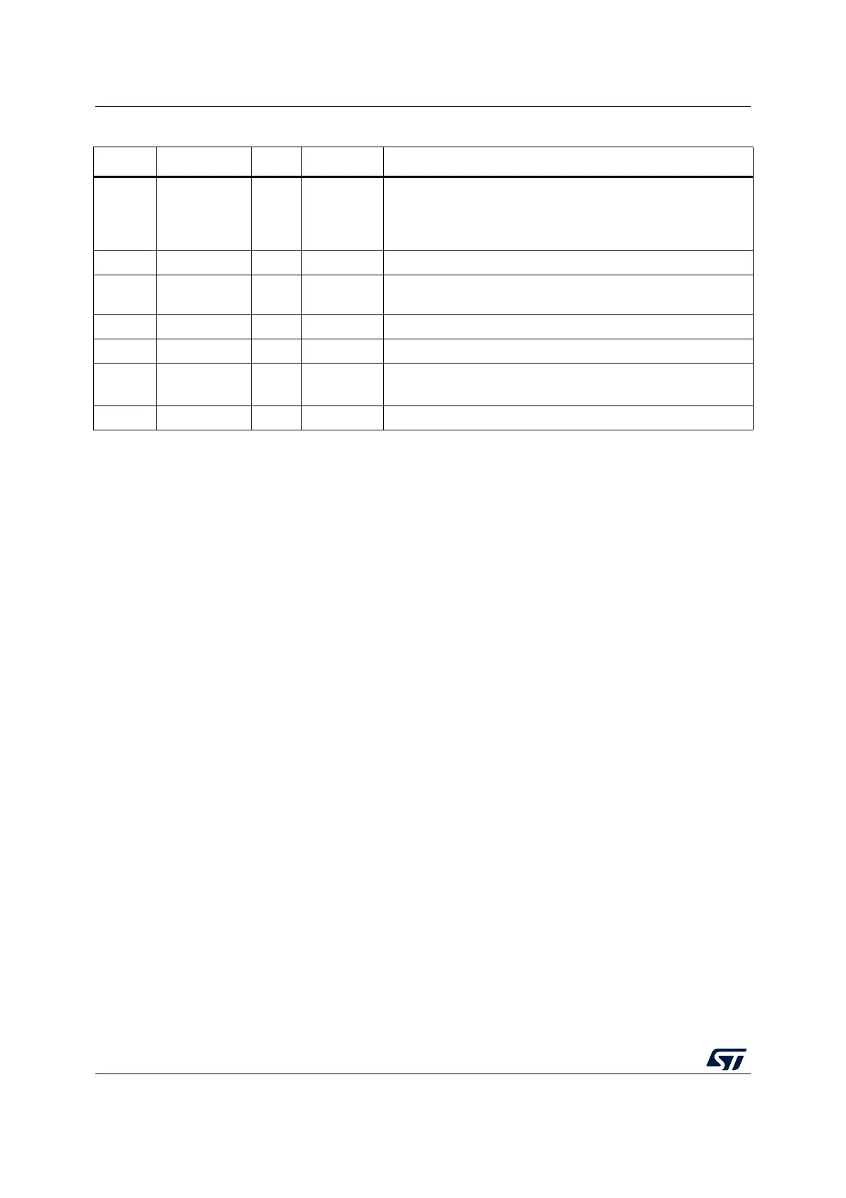
0x1C 0x1 3 AP_BD3R
Banked data 3 register (see Section 38.5.4)
Access to this register triggers a corresponding transaction on
the debug bus to the address in Address [31:4] = AP_TAR[31:4],
address [3:0] = 0xC.
0x20 - - - Reserved
0x24 to
0xEC
- - - Reserved
0xF0 - - - Reserved
0xF4 - - - Reserved
0xF8 0xF 2 AP_BASER
Debug base address register (RO) (see Section 38.5.5)
Base address of the ROM table
0xFC 0xF 3 AP_IDR Identification register (RO) (see Section 38.5.6)
Table 269. MEM-AP registers (continued)
Address APBANKSEL A(3:2) Name Description

 Loading...


