CMS32L051 User Manual |Chapter 5 Universal Timer Unit (Timer4)
www.mcu.com.cn 181 / 703
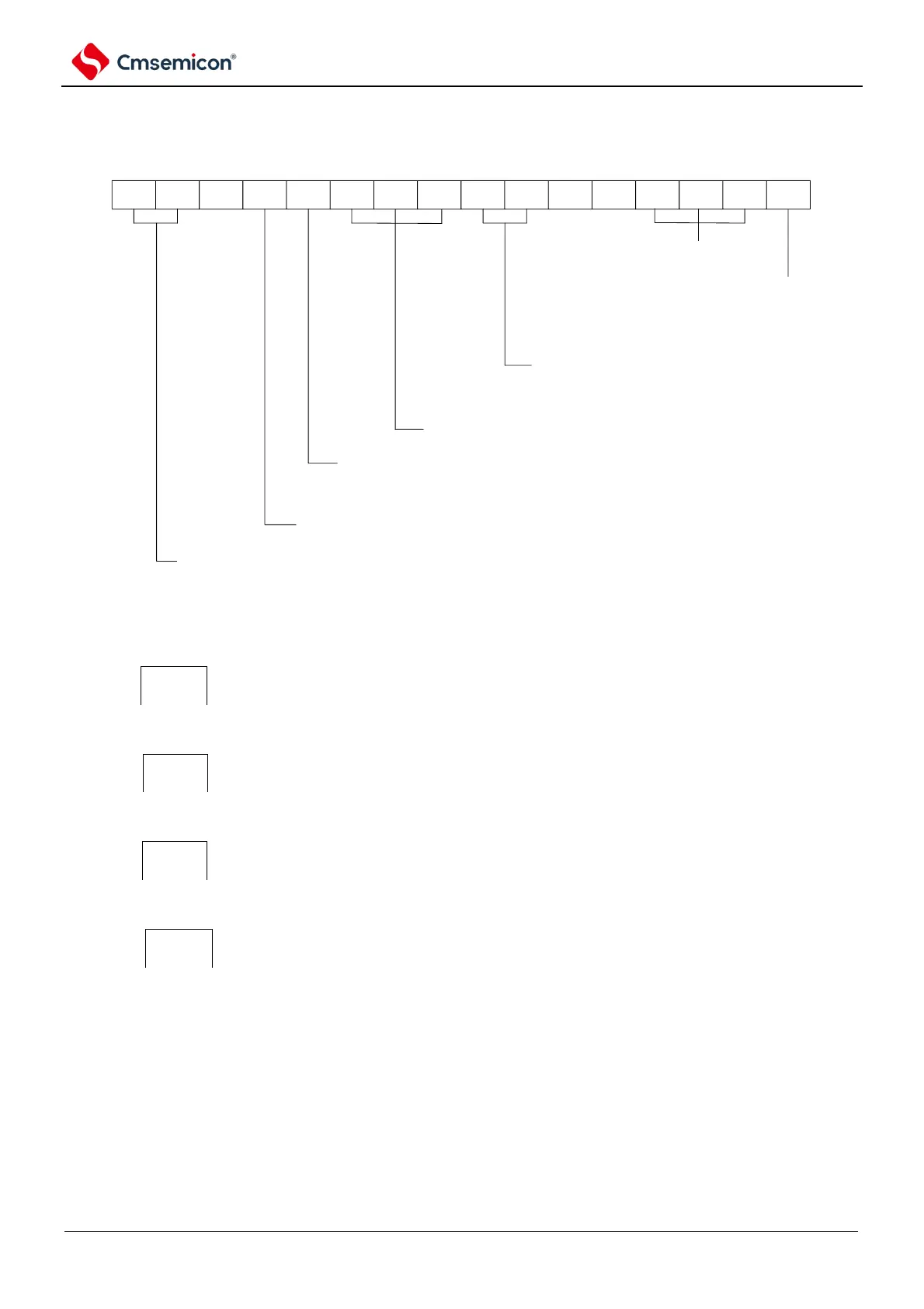
Figure 5-59 Example of register setting contents for delay counter function
(a) Timer mode register mn (TMRmn).
CKSmn1
1/0
CKSmn0
1/0
0
CCSmn
0
M/S
Note
0/1
STSmn2
0
STSmn1
0
STSmn0
1
CISmn1
1/0
CISmn0
1/0
0 0
MDmn3
1
MDmn2
0
MDmn1
0
MDmn0
1/0
14 13 12 11 10 9 8 7 6 5 4 3 2 1 015
TMRmn
operation mode of Channel N
100B : single counting mode
start trigger during operation
0: Trigger input invalid.
1: Trigger input valid.
start trigger selection
001B: Select Timn pin input valid edge
MASTERmnbit configuration (Channel 2)
0: Independent Channel operation
SPLITmn bit configuration (Channel 1, 3)
0: 16 bit Timer
Count clock selection
0: Select operational clock (fMCK)
operational clock (fMCK) selection
00B: select CKm0 as operational clock of Channel n
10B: select CKm1 as operational clock of Channel n.
01B: select CKm2 as operational clock of Channel 1,3.(only Channle 1,3 can select the value)
11B: select CKm3 as operational clock of Channel 1,3.(only Channle 1,3 can select the value)
Timn Pin input edge selection
00B: Detect falling edge
01B: Detect rising edge
10B: Detect both edges
11B: reserved
Note TMRm2: MASTERmn bit.
TMRm1, TMRm3: SPLITmn bit.
TMRm0: Fixed to 0.
Notem: Unit number (m=0) n: Channel number (n=0 ~ 3).