CMS32L051 User Manual |Chapter 5 Universal Timer Unit (Timer4)
www.mcu.com.cn 187 / 703
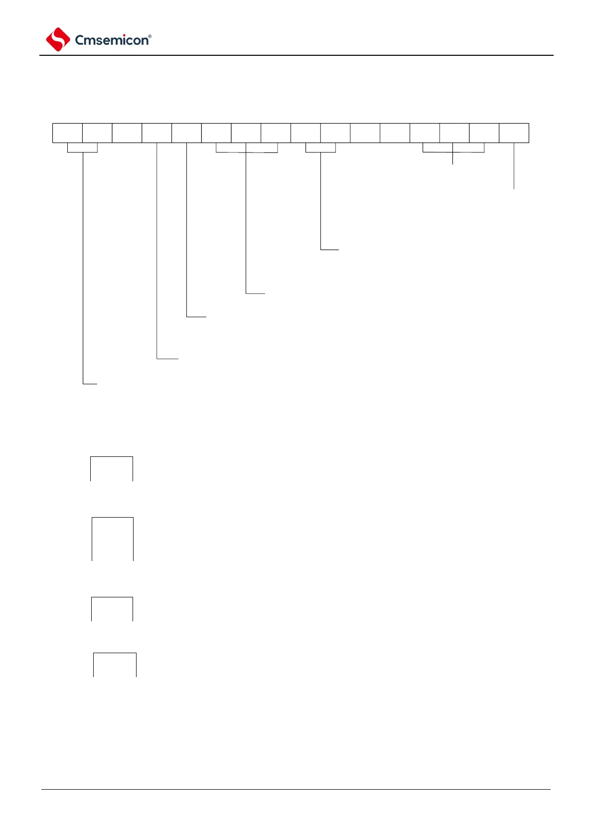
Figure 5-64 Example of register settings (slave channels) for single-trigger pulse output functions
(a) Timer mode register mp (TMRmp).
CKSmp1
1/0
CKSmp0
0
0
CCSmp
0
M/S
Note
0
STSmp2
1
STSmp1
0
STSmp0
0
CISmp1
0
CISmp0
0
0 0
MDmp3
1
MDmp2
0
MDmp1
0
MDmp0
0
14 13 12 11 10 9 8 7 6 5 4 3 2 1 015
TMRmp
operation mode of Channel P
100B: single counting mode
start trigger during operation
0: Trigger input invalid.
start trigger selection
100B: Select master control channel INTTMmn
MASTERmp bit configuration (Channel 2)
0: slave channel
SPLITmp bit configuration (Channel 1, 3)
0: 16 bit Timer
counting clock selection
0: Select operational clock (fMCK)
operational clock (fMCK) selection
00B: select CKm0 as operational clock of Channel p
10B: select CKm1 as operational clock of Channel p
same as master control channel configuration
TImp Pin input edge selection
00B: set to "00" since not used
(b) Timer output register m (TOm).
0: Output 0 by TOmp.
1: Output 1 by TOmp.
(c) The timer output enable register m (TOEm).
0: Stop TOmp output from counting
runs.
1: Enable TOmp output by counting
runs.
(d) Timer output level register m (TOLm).
0: Positive logic output (active high).
1: Negative logic output (active-low).
(e) Timer outputs mode register m (TOMm).
1: Set the slave channel output mode.
Note TMRm2: MASTERmp bit
TMRm1, TMRm3: SPLITmp bit
Note:m: Unit number (m= 0,1) n: master channel number (n=0, 2) p: slave channel number (n= 0: p=1, 2, 3, n=2: p=3)