CMS32L051 User Manual |Chapter 9 Clock output/Buzzer Output Controller
www.mcu.com.cn 254 / 703
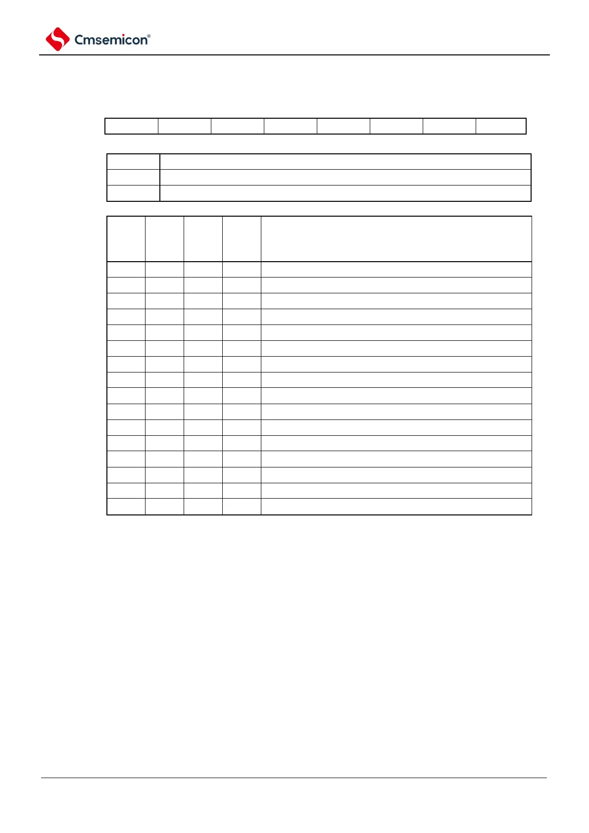
Figure 9-2 Format of clock output selection register n (CKSn)
Address: 0x40040FA5 (CKS0), 0x40040FA6 (CKS1) After reset: 00HR/W
Symbol
7 6 5 4 3 2 1 0
CKSn
Note The output clock must be used within the range of 16MHz. For details, please refer to AC characteristics of
the data sheet.
Note 1 The switching of the output clock must be made after the output is set to disable (PCLOEn=0).
2. When selecting the master system clock (CSELn=0), if you want to transfer to deep sleep mode, you must set
PCLOEn to 0 before executing WFI instructions; When the secondary system clock (CSELn=1) is selected,
because the RTCLPC bit of the mode control register (OSMC) can be supplied on the secondary system clock
with 0 and in deep sleep The clock is output in mode, so PCLOEn can be set to 1.
3. When the RTCLPC bit of the Mode Control Register (OSMC) of the subsystem clock is 1 and the CPU is
running at the secondary system clock (f
SUB
). In sleep mode, the secondary system clock (f
SUB
) cannot be
output from the CLKBUZn pin.
Note 1. n =0, 1
2. f
MAIN:
Main system clock frequency
f
SUB:
Subsystem clock frequency