CMS32L051 User Manual |Chapter 11 A/D Converter
www.mcu.com.cn 273 / 703
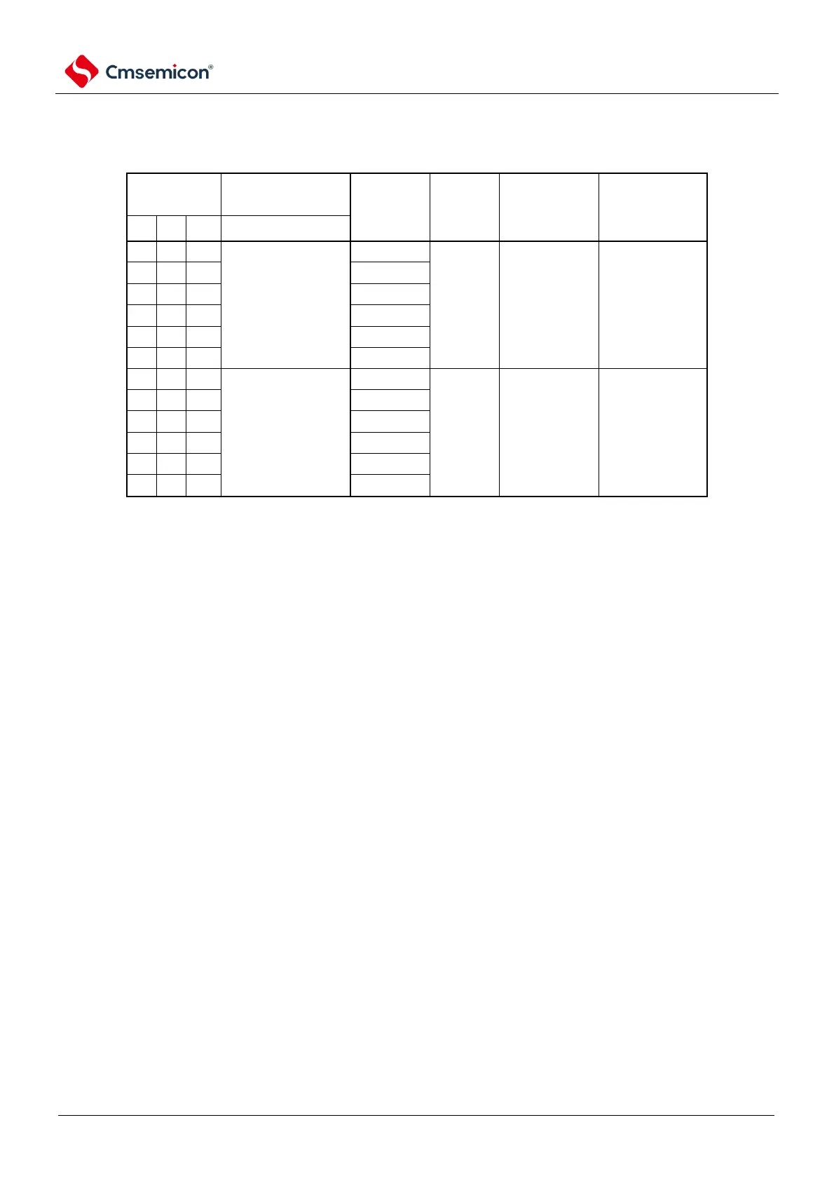
Table11-4 A/D conversion times (2/2)
(2) There is an A/D power stabilization wait time (hardware triggered wait mode
Note 1
).
Notice 1. When the hardware trigger wait mode, the power supply settling time is guaranteed by the hardware design
and does not need to be set. And in continuous conversion mode, the A/D power stabilization wait time occurs only
after the hardware trigger is detected for the first time.
Notice 2. Time required for ADC conversion after hardware triggering = 2us + (number of sample clocks + number of
successive comparison clocks)/fAD
The number of sample clocks can be adjusted via the ADSMPWAIT register, which defaults to four ADCLK.
The fastest clock supported by ADCLK is 8MHz.
Note 1. To override the FR2~FR0 bits and ADSMPWAIT bits into different data, it must be done in the transition stop
state (ADCS=0).
2. The transition time in the hardware-triggered wait mode includes the A/D power stabilization wait time after the
hardware trigger is detected.
Remark fCLK: Clock frequency of the CPU/peripheral hardware