CMS32L051 User Manual |Chapter 11 A/D Converter
www.mcu.com.cn 272 / 703
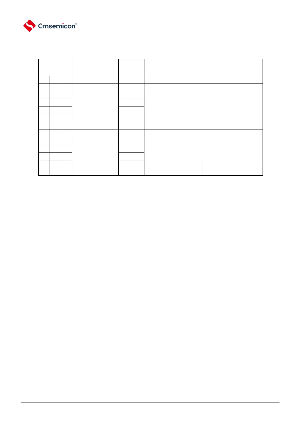
Table 11-3 A/D conversion time (1/2)
(1) No A/D power stabilization wait time (software trigger mode/hardware trigger no wait mode).
A/D converter
mode register 0
(ADM0)
A/D sampling time
extension
register (ADSMPWAIT)
Convert
frequency of
clock ADCLK
(f
AD
)
12-bit resolution conversion time
Note 2
ADC conversion time = (number of sample clocks + number of
successive comparison clocks)/ fAD
Number of ADC conversion clocks
16 ADCLK
(4 sample clocks +12 successive
comparison clocks).
20 ADCLK
(8 sample clocks +12 successive
comparison clocks).
Note 1: To override the FR2~FR0 bits and ADSMPWAIT bits into different data, it must be done in the transition stop
state (ADCS=0).
Note 2. Time required for an ADC conversion = (number of sample clocks + number of successive comparison clocks)/
fAD
The number of sample clocks can be adjusted via the ADSMPWAIT register, which defaults to four ADCLK.
The fastest clock supported by ADCLK is 8MHz.
Note fCLK: The clock frequency of the CPU/peripheral hardware
fAD: The ADC converts the clock frequency up to 8MHz.