CMS32L051 User Manual |Chapter 14 Serial interface IICA
www.mcu.com.cn 483 / 703
(2) Slave address register n (SVAn)
This is the register that holds the 7-bit local station address {A6, A5, A4, A3, A2, A1, A0} when used as a
slave.
The SVAn register is set via an 8-bit memory operation command. However, when the STDn bit is 1
(start condition detected), overriding this register is prohibited.
After the reset signal is generated, the value of this register becomes 00H.
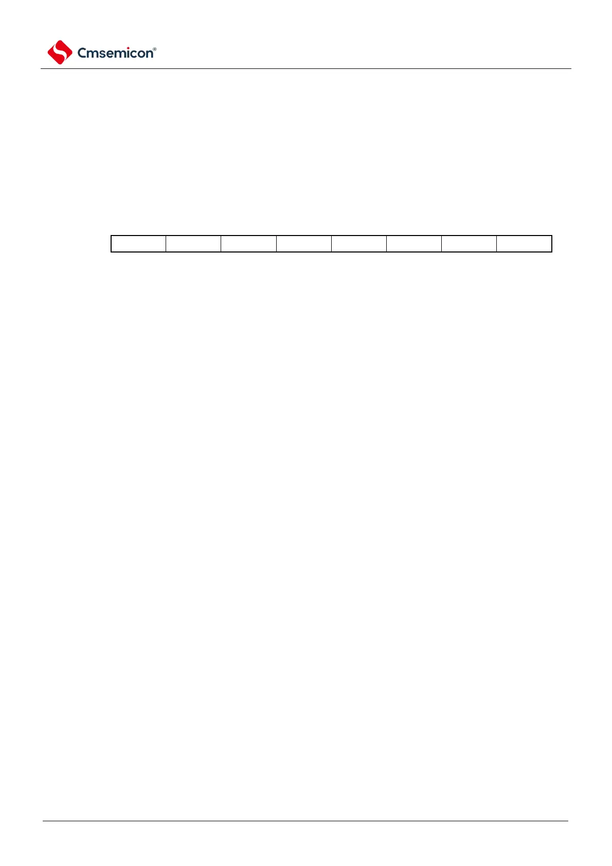
Figure 14-4 Format of dependent address register n (SVAn)
Address: 0x40041A34 After reset: 00HR/W
Symbol
7 6 5 4 3 2 1 0
SVAn
Note Bit0 is fixed as 0.
(3) SO latch
The SO latch maintains the output level of the SDAAn pin.
(4) Wake up control circuitry
This circuit generates an interrupt request (INTIICAn) when the address value set in the slave address
register n (SVAn) is the same as the received address or when the extension code is received.
(5) Serial clock counter
During transmit or receive, this counter counts the serial clock of the output or input and checks whether
8-bit data has been transmitted and received.
(6) Interrupt request signal generation circuit
This circuit control generates an interrupt request signal (INTIICAn). An I
2
C interrupt request is generated
by the following two triggers.
Drop of the 8th or 9th serial clock (set by WTIMn bit).
Interrupt request due to detection of a stop condition (set via SPIEn bit).
Note WTIMn bit: Bit3 of IICA control register n0
(IICCTLn0).
SPIE nbit : Bit4 of IICA control register n0
(IICCTLn0).
(7) Serial clock control circuitry
In master mode, this circuit generates the output clock from the sample clock to the SCLAn pin.
(8) Serial clock wait control circuitry
This circuit controls the wait timing.