CMS32L051 User Manual |Chapter 22 Power-On Reset Circuit
www.mcu.com.cn 646 / 703
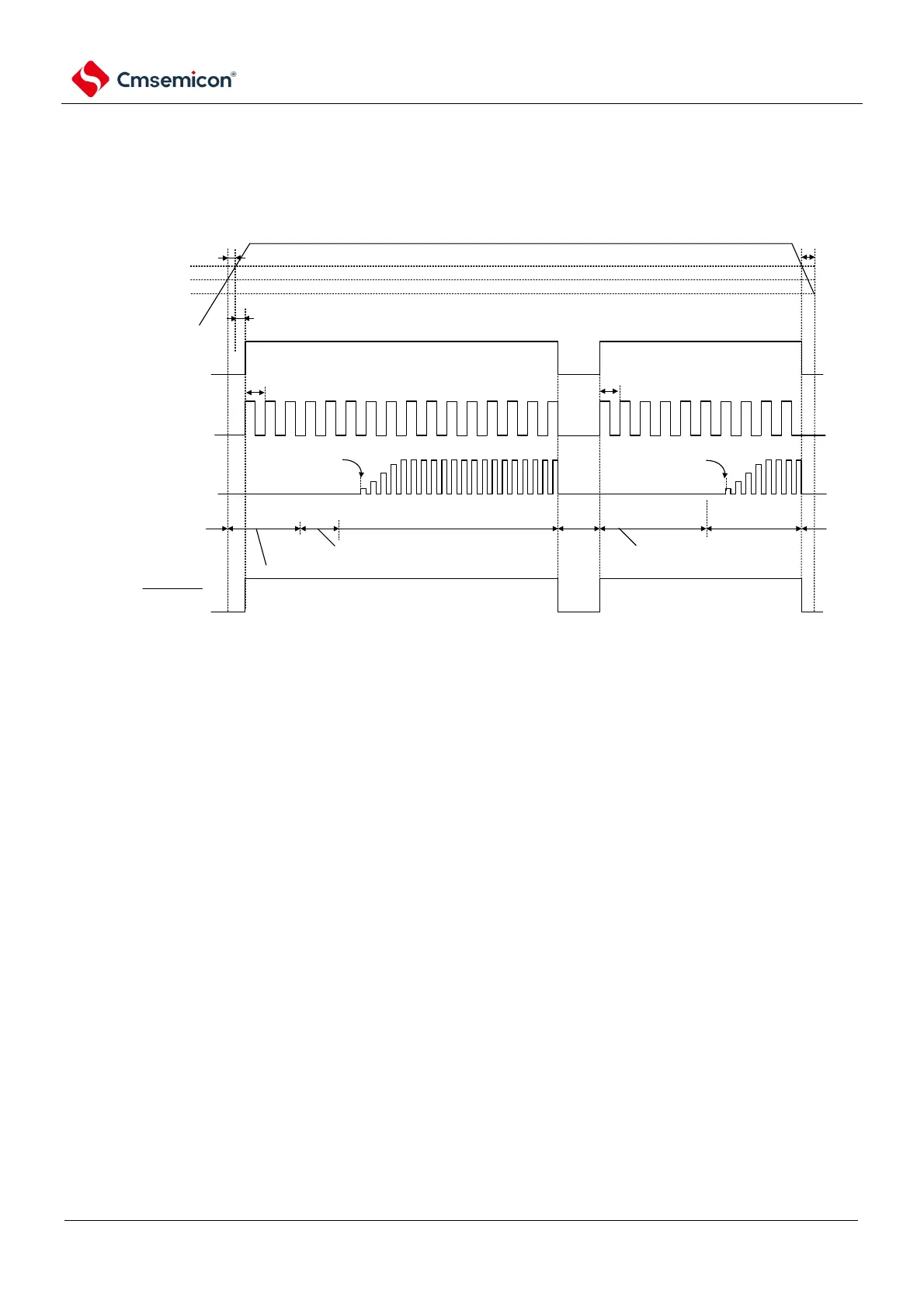
Figure 22-2 Timing of internal reset signal generation for power-on reset circuit and voltage detection
circuit (1/3)
(1) A case of using an external reset input on the RESETB pin
low limit of working
voltage range
VPOR=1.51V(TYP.)
VPDR=1.50V(TYP.)
note 5 note 5
at least 10us
wait till osc precision
stablized
note 1
wait till osc precision
stablized
note 1
start oscillating via
software configuration
start oscillating via
software configuration
power supply
voltage(VDD)
0V
RESETB pin
high speed internal
osc clock(fIH)
high speed system clock
(fMX)
(Scenario of selecting
X1 oscilation)
stop operation
CPU
wait time of voltage stablization
reset processing time while
releasing external reset
note 3
normal operation
(high speed internal osc clock)
note 2
normal operation
(high speed internal osc clock)
not
e 2
reset processing time while
releasing external reset
note 3
reset period
(osc stop)
internal reset signal
stop
operation
Note 1 The internal reset processing time includes the oscillation accuracy stabilization wait time for the high-speed
internal oscillator clock.
2. Ability to switch the CPU clock from a high-speed internal oscillator clock to a high-speed system clock or a sub-
system clock. In the case of an X1 clock, the switching must be made after confirming the oscillation settling time
through the status register (OSTC) of the oscillation settling time counter; In the case of an XT1 clock, the switching
must be made after confirming the oscillation settling time using the timer function, etc.
3. When the supply voltage rises, the reset state must be maintained by external reset before the supply voltage
reaches the operating voltage range shown in the AC characteristics of the data sheet; When the supply voltage
drops, it must be reset through deep sleep mode transfer, voltage detection circuitry, or external reset before the
supply voltage falls below the operating voltage range. During restart operation, it must be confirmed that the supply
voltage returns to the operating voltage range.
Note V
POR
: The POR supply voltage rises to detect the voltage
V
PDR
: The POR supply voltage drops the detection voltage
Notice When the LVD is OFF, an external reset of the RESET B pin must be used. For details, please refer to Chapter
23 Voltage Detection Circuits.