CMS32L051 User Manual |Chapter 22 Power-On Reset Circuit
www.mcu.com.cn 647 / 703
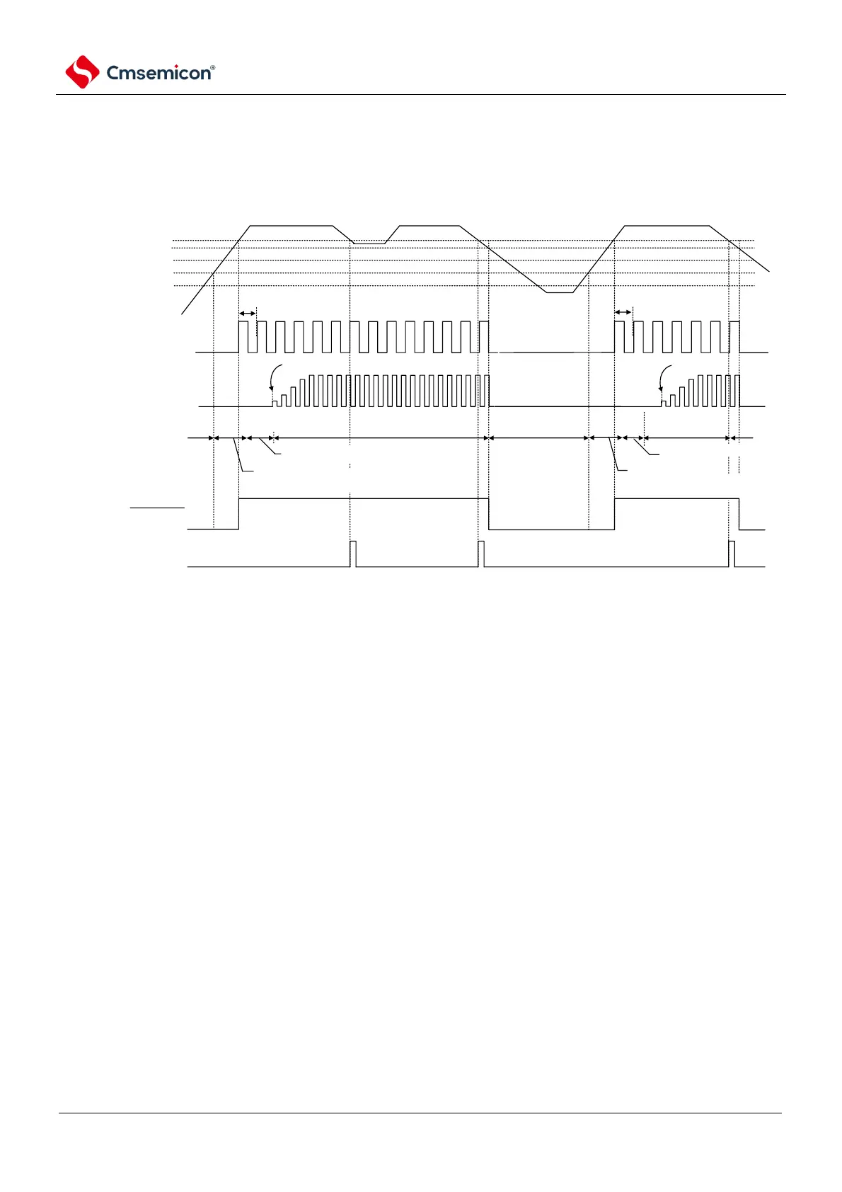
Figure 22-2 Timing of internal reset signal generation for power-on reset circuit and voltage detection
circuit (2/3)
(2) LVD is in interrupt & reset mode (option bytes 000C1H LVIMDS1, LVIMDS0=1, 0).
low limit of working
voltage range
VPOR=1.51V(TYP.)
VPDR=1.50V(TYP.)
wait till osc precision
stablized
note1
wait till osc precision
stablized
note1
start oscillating via
software configuration
start oscillating via software
configuration
power supply
voltage(VDD)
0V
high speed internal
osc clock(fIH)
high speed system clock
(fMX) (Scenario of
selecting X1 oscilation)
stop
operation
CPU
reset period
(osc stop)
internal reset signal
stop
operation
VLVDL
VLVDH
normal operation (high speed
internal osc clock)
note2
wait time of voltage stablization + POR
reset processing time
1.64ms(TYP), 3.10ms(MAX).
wait time of voltage stablization + POR reset
processing time
LVD reset processing time
Note4
LVD reset
processing time
INTLVI
Note3
normal operation (high speed
internal osc clock)
note2
Note 1. The internal reset processing time includes the oscillation accuracy stabilization wait time for the high-speed
internal oscillator clock.
2. Ability to switch the CPU clock from a high-speed internal oscillator clock to a high-speed system clock or a sub-
system clock. In the case of an X1 clock, the switching must be made after confirming the oscillation settling time
through the status register (OSTC) of the oscillation settling time counter; In the case of an XT1 clock, the switching
must be made after confirming the oscillation settling time using the timer function, etc.
3. After generating the interrupt request signal (INTLVI), the LVILV bit and the LVIMD bit of the voltage detection level
register (LVIS) are automatically set to "1". Therefore, it must be considered that the supply voltage may return to
the high voltage detection voltage (VLVDH) or higher without falling below the low voltage detection voltage
3-8 Setting procedure for confirmation/reset of
3-9
4. In addition to the "voltage stabilization wait + POR reset process" after reaching VPOR (1.51V(TYP.)), the following
"LVD reset process" is required after reaching the LVD detection level (VLVDH) until the start of normal operation ".
Note V
LVDH
, V
LVDL
:
LVD sense voltage
V
POR
: POR supply voltage rise detection voltage
V
PDR
: POR supply voltage drop detection voltage