CMS32L051 User Manual |Chapter 22 Power-On Reset Circuit
www.mcu.com.cn 648 / 703
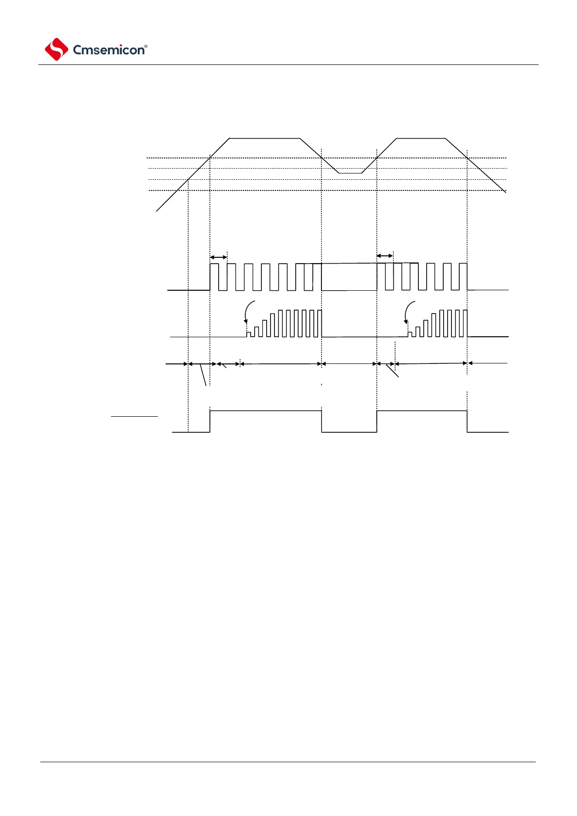
Figure 22-2 Timing of internal reset signal generation for power-on reset circuit and voltage detection
circuit (3/3)
(3) LVD reset mode case (option byte 000C1H LVIMDS1, LVIMDS0=1, 1).
low limit of working
voltage range
VPOR=1.51V(TYP.)
VPDR=1.50V(TYP.)
power supply
voltage(VDD)
0V
high speed internal osc
clock(fIH)
high speed system clock
(fMX) (Scenario of selecting
X1 oscilation)
stop
operation
CPU
internal reset signal
VLVD
wait time of voltage stablization + POR reset
processing time
wait till osc precision
stablized
note1
wait till osc precision
stablized
note1
start oscillating via
software configuration
start oscillating via
software configuration
normal operation (high speed
internal osc clock)
note2
normal operation (high speed
internal osc clock)
note2
reset period
(osc stop)
reset period
(osc stop)
LVD reset processing time
note3
LVD reset processing time
note3
Note 1 The internal reset processing time includes the oscillation accuracy stabilization wait time for the high-speed
internal oscillator clock.
2. Ability to switch the CPU clock from a high-speed internal oscillator clock to a high-speed system clock or a sub-
system clock. In the case of an X1 clock, the switching must be made after confirming the oscillation settling time
through the status register (OSTC) of the oscillation settling time counter; In the case of an XT1 clock, the switching
must be made after confirming the oscillation settling time using the timer function, etc.
3. The time to start running normally except to reach VPOR (1.51V (TYP.). In addition to voltage stabilization waiting
+POR reset processing, it is required after the LVD detection level (V
LVD
) is reached LVD Reset Processing.
4. When the supply voltage drops, if the supply voltage is restored only after the internal reset of the voltage detection
circuit (LVD), the LVD reset process is required after the LVD sense level (V
LVD
) is reached
Note 1 V
LVDH
, V
LVDL
:
LVD sense voltage
V
POR
: The POR supply rises the sense voltage
V
PDR
: The POR supply drops the sense voltage
2. When the LVD interrupt mode is selected (option bytes 000C1H LVIMD1, LVIMD0=0, 1), the time from power-on
to start the usual operation is the same as the time in Note 3 of Figure LVD Reset Mode.