CMS32L051 User Manual |Chapter 23 Voltage Detection Circuit
www.mcu.com.cn 666 / 703
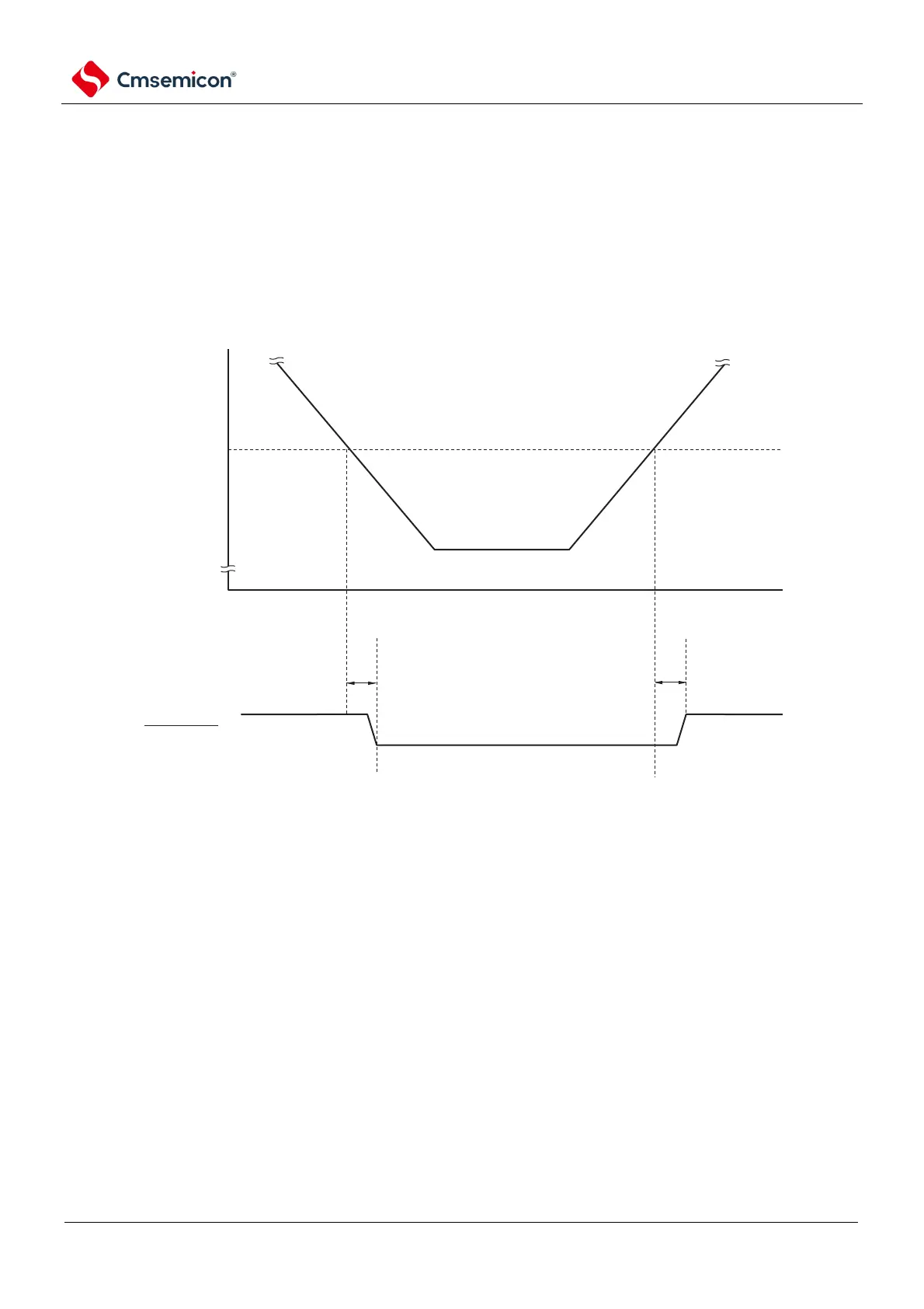
(2) The delay from the generation of the LVD reset source to the generation or release of the LVD reset
From meeting the supply voltage (V
DD
)<LVDDetection voltage (V
LVD
) to generate LVDA delay
occurs until the reset. Again, from LVD Detection voltage (V
LVD
DD
) to Dismiss LVDA
delay can also occur until the reset (reference
Figure 23-10).
Figure 23-10 Delay from generation of LVD reset source to generation or release of LVD reset
① : Detection delay (300us (MAX.)).
(3) For situations where LVD is plugged in when LVD is set to OFF
When setting the LVD to OFF, an external reset of the RESET B pin must be used.
During an external reset, a low level of at least 10us must be entered into the RESETB pin. If an
external reset is performed when the supply voltage rises, the supply must be turned on after entering low
on the RESETB pin and at least 10us low over the operating voltage range shown in the AC characteristics
of the data sheet, and then enter high.
(4) The operating voltage drops when LVD is set to OFF and set to LVD interrupt mode
With LVD set to OFF and set to LVD interrupt mode, if the operating voltage drops, it must be reset
by transfer from deep sleep mode or external reset before the operating voltage drops below the operating
voltage range shown in the AC characteristics of the data sheet. During restart operation, it must be
confirmed that the supply voltage returns to the operating voltage range.