USB on-the-go full-speed/high-speed (OTG_FS/OTG_HS) RM0390
1098/1328 RM0390 Rev 4
consumption due to the USB clock switching activity is cut even if the system clock is
kept running by the application for other purposes.
• USB system stop
When the OTG_FS/OTG_HS is in the USB suspended state, the application may
decide to drastically reduce the overall power consumption by a complete shut down of
all the clock sources in the system. USB System Stop is activated by first setting the
Stop PHY clock bit and then configuring the system deep sleep mode in the power
control system module (PWR).
The OTG_FS/OTG_HS core automatically reactivates both system and USB clocks by
asynchronous detection of remote wakeup (as an host) or resume (as a device)
signaling on the USB.
To save dynamic power, the USB data FIFO is clocked only when accessed by the
OTG_FS/OTG_HS core.
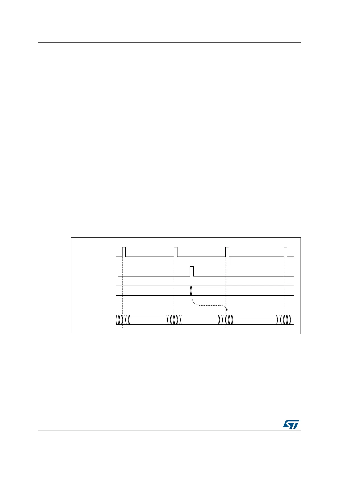
31.10 Dynamic update of the OTG_HFIR register
The USB core embeds a dynamic trimming capability of micro-SOF[HS] / SOF[FS] framing
period in host mode allowing to synchronize an external device with the micro-SOF[HS] /
SOF[FS] frames.
When the OTG_HFIR register is changed within a current micro-SOF[HS] / SOF[FS] frame,
the SOF period correction is applied in the next frame as described in Figure 406.
For a dynamic update, it is required to set RLDCTRL=0.
Figure 406. Updating OTG_HFIR dynamically (RLDCTRL = 0)
31.11 USB data FIFOs
The USB system features 1.25[FS] / 4[HS] Kbytes of dedicated RAM with a sophisticated
FIFO control mechanism. The packet FIFO controller module in the OTG_FS/OTG_HS core
organizes RAM space into Tx FIFOs into which the application pushes the data to be
temporarily stored before the USB transmission, and into a single Rx FIFO where the data
received from the USB are temporarily stored before retrieval (popped) by the application.
The number of instructed FIFOs and how these are organized inside the RAM depends on
DLE
62)UHORDG
27*B+),5ZULWH
27*B+),5YDOXH
)UDPHWLPHU
 Loading...


