Secure digital input/output interface (SDIO) RM0390
984/1328 RM0390 Rev 4
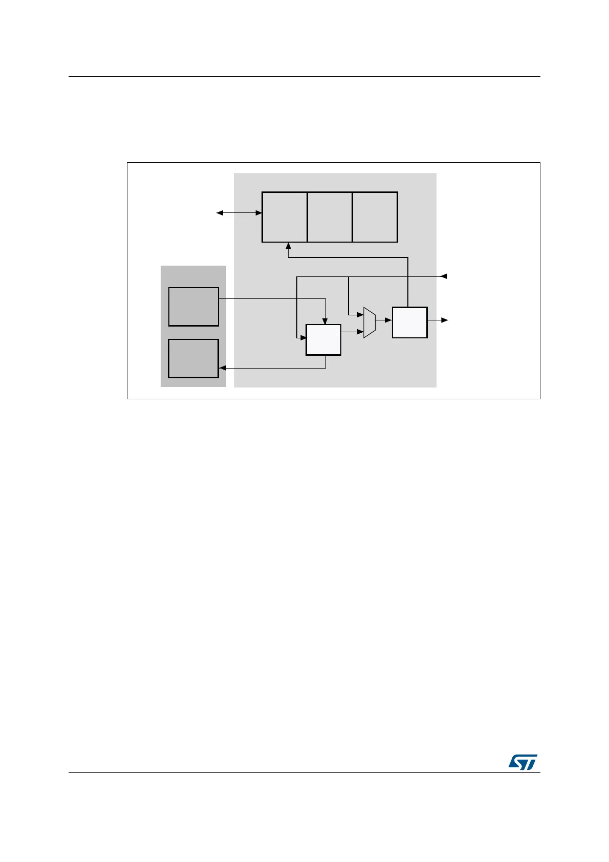
Data path
The data path subunit transfers data to and from cards. Figure 382 shows a block diagram
of the data path.
Figure 382. Data path
The card databus width can be programmed using the clock control register. If the 4-bit wide
bus mode is enabled, data is transferred at four bits per clock cycle over all four data signals
(SDIO_D[3:0]). If the 8-bit wide bus mode is enabled, data is transferred at eight bits per
clock cycle over all eight data signals (SDIO_D[7:0]). If the wide bus mode is not enabled,
only one bit per clock cycle is transferred over SDIO_D0.
Depending on the transfer direction (send or receive), the data path state machine (DPSM)
moves to the Wait_S or Wait_R state when it is enabled:
• Send: the DPSM moves to the Wait_S state. If there is data in the transmit FIFO, the
DPSM moves to the Send state, and the data path subunit starts sending data to a
card.
• Receive: the DPSM moves to the Wait_R state and waits for a start bit. When it
receives a start bit, the DPSM moves to the Receive state, and the data path subunit
starts receiving data from a card.
Data path state machine (DPSM)
The DPSM operates at SDIO_CK frequency. Data on the card bus signals is synchronous to
the rising edge of SDIO_CK. The DPSM has six states, as shown in Figure 383: Data path
state machine (DPSM).
06Y9
'DWDSDWK
'DWD),)2
7UDQVPLW
6WDWXV
IODJ
&5&
6KLIW
UHJLVWHU
7RFRQWUROXQLW
6',2B'LQ>@
6',2B'RXW>@
5HFHLYH
&RQWURO
ORJLF
'DWD
WLPHU